Port Diagram
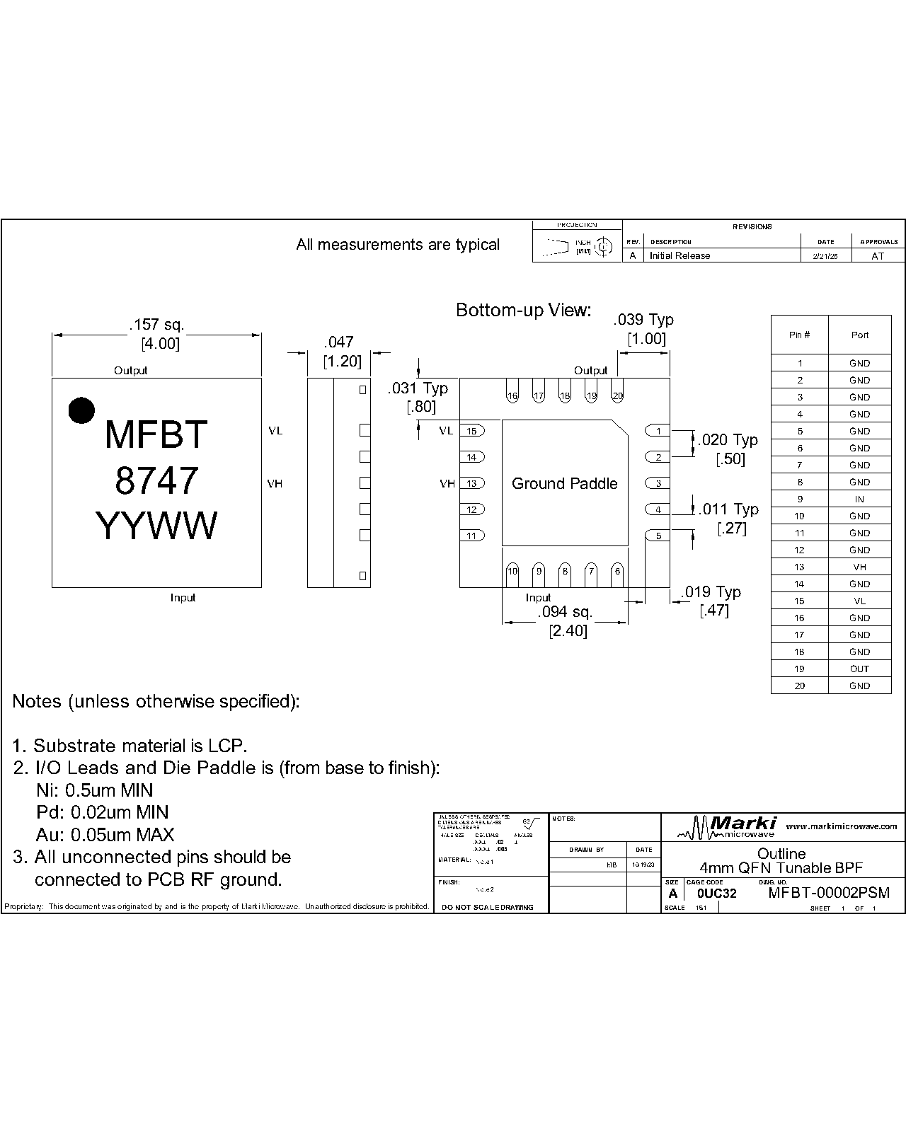
A top-down x-ray view of the MFBT-00002PSM package outline drawing is shown below. The MMIC bandpass filters are symmetrical allowing Pin 9 or Pin 19 to be used as the input.

Sales: 408-778-9952 | General: 408-778-4200 | Fax: 408-778-4300
Sales & Customer Support: [email protected]
Tech Support: [email protected]
The MFBT-00002PSM is a surface mount MMIC tunable filter for adaptive filtering applications. The MFBT-00002PSM offers separate low pass and high pass tuning capability, allowing users to create bandpass filters with variable center frequencies and % bandwidths. Performance features include low return loss in both the passband and stopband and low insertion loss, high stopband rejection, and high IP3 relative to other tunable filters. The MFBT-00002PSM is available as a 4x4mm plastic QFN, replacing much larger switched filter banks.

| Part Number | Description | Package | Green Status | Product Lifecycle | Export Classification |
|---|---|---|---|---|---|
| MFBT-00002PSM | GaAs MMIC 4.5 - 16.5 GHz Tunable Filter | QFN | REACH RoHS | Released | 3A001.b.5.a |
| EVB-MFBT-00002P | GaAs MMIC 4.5 - 16.5 GHz Tunable Filter | EVB | REACH RoHS | Released | 3A001.b.5.a |
MFBT-00002PSM
GaAs MMIC 4.5 - 16.5 GHz Tunable Filter
| Revision Code | Revision Date | Comment |
|---|---|---|
| - | 2023-12-05 | Datasheet Initial Release |
MFBT-00002PSM
GaAs MMIC 4.5 - 16.5 GHz Tunable Filter
A top-down x-ray view of the MFBT-00002PSM package outline drawing is shown below. The MMIC bandpass filters are symmetrical allowing Pin 9 or Pin 19 to be used as the input.
| Port | Function | Description | DC Equivalent Circuit |
|---|---|---|---|
| Pin 13 | VH | Pin 13 sets the high pass cutoff frequency tuning voltage and is diode connected and matched to 50Ω. The high pass cutoff frequency increases with increasing voltage. |  |
| Pin 15 | VL | Pin 15 sets the low pass cutoff frequency tuning voltage and is diode connected and matched to 50Ω. The low pass cutoff frequency increases with increasing voltage. | |
| Pin 19 | Output | Pin 19 is connected to ground through an RC network with a large resistor value and matched to 50Ω. |  |
| Pin 9 | Input | Pin 9 is connected to ground through an RC network with a large resistor value and matched to 50Ω. | |
MFBT-00002PSM
GaAs MMIC 4.5 - 16.5 GHz Tunable Filter
The Absolute Maximum Ratings indicate limits beyond which damage may occur to the device. All limits are individual and should not be met in parallel, doing so will degrade the lifetime of the device. If these limits are exceeded, the device may be inoperable or have a reduced lifetime.
| Parameter | Maximum Rating | Unit |
|---|---|---|
| Maximum Operating Temperature | 85 | °C |
| Maximum Storage Temperature | 125 | °C |
| Minimum Operating Temperature | -55 | °C |
| Minimum Storage Temperature | -65 | °C |
| Power Handling, at any Port | 36 | dBm |
| Parameter | Details | Rating |
|---|---|---|
| Dimensions | - | 4 x 4 mm |
| Moisture Sensitivity Level | - | MSL 1 |
The Recommended Operating Conditions indicate the limits, inside which the device should be operated, to guarantee the performance given in Electrical Specifications Operating outside these limits may not necessarily cause damage to the device, but the performance may degrade outside the limits of the electrical specifications. For limits, above which damage may occur, see Absolute Maximum Ratings.
| Parameter | Min | Nominal | Max | Unit |
|---|---|---|---|---|
| VL Tuning Voltage | 0 | - | 16 | V |
| VH Tuning Voltage | 0 | - | 16 | V |
MFBT-00002PSM
GaAs MMIC 4.5 - 16.5 GHz Tunable Filter
The electrical specifications apply at TA=+25°C in a 50Ω system. Typical data shown is for the filter in a PSM package with a sine wave input applied to Pin 9. Bias voltage is VL/VH unless otherwise specified. Min and Max limits are guaranteed at TA=+25°C.
| Parameter | Test Conditions | Minimum Frequency (GHz) | Maximum Frequency (GHz) | Min | Typ | Max | Unit |
|---|---|---|---|---|---|---|---|
| Center Freq | - | - | - | 5.5 | - | 15.5 | GHz |
| Highside Rejection at 1.5*fc | - | - | - | - | 35 | - | dB |
| Impedance | - | - | - | - | 50 | - | Ω |
| Insertion Loss @ fc | - | 5.5 | 15.5 | - | 6.5 | - | dB |
| Lowside Rejection at 0.4*fc | - | - | - | - | 35 | - | dB |
| Output IP3 | - | - | - | - | 33 | - | dBm |
| Passband Return Loss | - | 4.5 | 16.5 | - | 15 | - | dB |
| Tunable 3dBc Passband | - | - | - | 4.5 | - | 16.5 | GHz |
| Tuning Voltage - VH, VL | - | - | - | 0 | - | 16 | V |
| - | 8V/8V | - | - | - | 34 | - | dBm |
MFBT-00002PSM
GaAs MMIC 4.5 - 16.5 GHz Tunable Filter
Specifications guaranteed from -55 to +85°C, measured in a 50-Ohm system. All plots are deembedded to the device pads unless otherwise noted.


MFBT-00002PSM
GaAs MMIC 4.5 - 16.5 GHz Tunable Filter

OIP3 measured on evaluation board with losses embedded
MFBT-00002PSM
GaAs MMIC 4.5 - 16.5 GHz Tunable Filter
MFBT-00002PSM
GaAs MMIC 4.5 - 16.5 GHz Tunable Filter
Download : Footprint Drawing

MFBT-00002PSM
GaAs MMIC 4.5 - 16.5 GHz Tunable Filter