Absolute Maximum Ratings
| Parameter | Maximum Rating | Unit |
|---|---|---|
| Maximum Operating Temperature | 100 | °C |
| Maximum Storage Temperature | 125 | °C |
| Minimum Operating Temperature | -55 | °C |
| Minimum Storage Temperature | -65 | °C |
| RF Power Handling | 37 | dBm |
Sales: 408-778-9952 | General: 408-778-4200 | Fax: 408-778-4300
Sales & Customer Support: [email protected]
Tech Support: [email protected]
The MBALH-0R520CSP2 is a GaAs passive MMIC 1:1 balun that features excellent 32 dB common mode rejection over a 0.5 to 20 GHz operational bandwidth. The MBALH-0R520CSP2 is footprint compatible with the 2:1 MBAL-0R520CSP2, offering flexibility in system design. For ADC and DAC interface applications, the choice between the 1:2 and 1:1 configurations will depend on specific system requirements. This device is an ideal solution for digital beamforming and other higher-order Nyquist sampling applications, as well as clock distribution and balanced amplifier interfaces. Available in a lead-free, RoHS compliant 2.5 x 2.5 mm CSP2 package, it is compatible with standard pick-and-place assembly processes.

| Part Number | Description | Package | Green Status | Product Lifecycle | Export Classification |
|---|---|---|---|---|---|
| MBALH-0R520CSP2 | 0.5-20 GHz Passive MMIC Chip Scale Package 1:1 Balun | CSP2 | REACH RoHS | Released | EAR99 |
| EVB-MBALH-0R520 | Evaluation Board, 0.5-20 GHz Passive MMIC Chip Scale Package 1:1 Balun | EVB | REACH RoHS | Released | EAR99 |
MBALH-0R520CSP2
0.5-20 GHz Passive MMIC Chip Scale Package 1:1 Balun
| Revision Code | Revision Date | Comment |
|---|---|---|
| - | 2025-04-21 | Initial Release |
| A | 2025-04-28 | Updated Moisture Sensitivity from MSL3 to MSL1 |
| B | 2026-04-23 | Updated RF Power Handling |
| C | 2026-06-03 | Updated Port Description |
MBALH-0R520CSP2
0.5-20 GHz Passive MMIC Chip Scale Package 1:1 Balun
| Port | Function | Description | DC Equivalent Circuit |
|---|---|---|---|
| GND | Ground | Ground pad should be connected to RF/DC ground with low electrical and thermal resistance. |  |
| Pin 1 | Common Port / In (Unbalanced) | The common port is DC short to ground. |  |
| Pin 3 | Out 1 / 0° Port (Balanced) | The 0° port is DC short to ground. | |
| Pin 4 | Out 2 / 180° Port (Balanced) | The 180° port is DC open. | |
| Pins 2,5 | NC | Pins 2 and 5 are not internally connected. They can be connected to ground for normal operation. |  |
MBALH-0R520CSP2
0.5-20 GHz Passive MMIC Chip Scale Package 1:1 Balun
| Parameter | Maximum Rating | Unit |
|---|---|---|
| Maximum Operating Temperature | 100 | °C |
| Maximum Storage Temperature | 125 | °C |
| Minimum Operating Temperature | -55 | °C |
| Minimum Storage Temperature | -65 | °C |
| RF Power Handling | 37 | dBm |
| Parameter | Details | Rating |
|---|---|---|
| ESD | 250 to < 500 Volts | HBM Class 1A |
| Dimensions | - | 2.50 x 2.50 mm |
| Moisture Sensitivity Level | - | MSL 1 |
MBALH-0R520CSP2
0.5-20 GHz Passive MMIC Chip Scale Package 1:1 Balun
| Parameter | Test Conditions | Minimum Frequency (GHz) | Maximum Frequency (GHz) | Min | Typ | Max | Unit |
|---|---|---|---|---|---|---|---|
| Amplitude Balance | 25°C | 0.5 | 20 | - | 0.3 | - | dB |
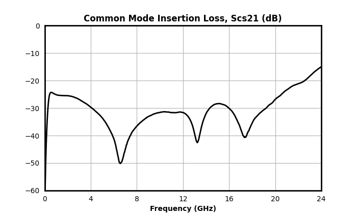
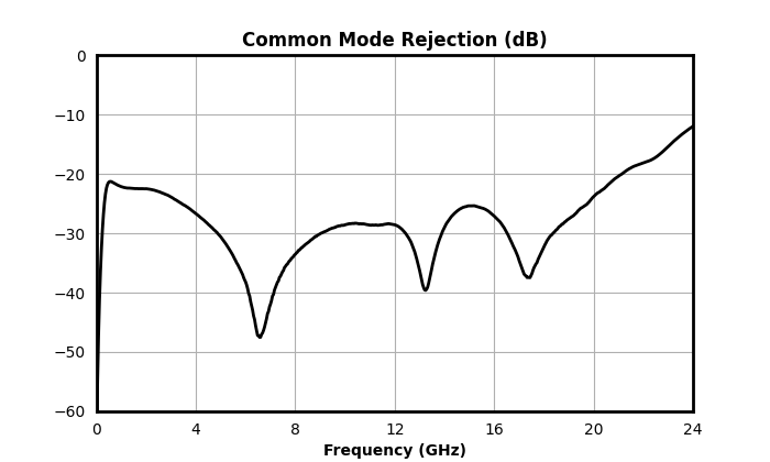
| Common Mode Rejection | 25°C | 0.5 | 20 | - | 32 | - | dB |
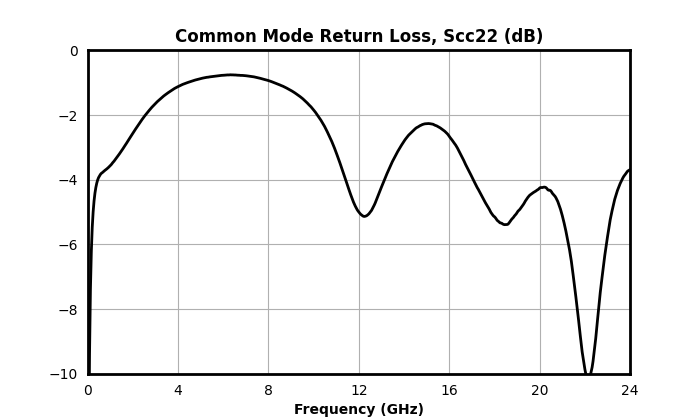
| Common Port Return Loss | 25°C | 0.5 | 20 | - | 16 | - | dB |
| Impedance | 25°C | 0.5 | 20 | - | 50 | - | Ω |
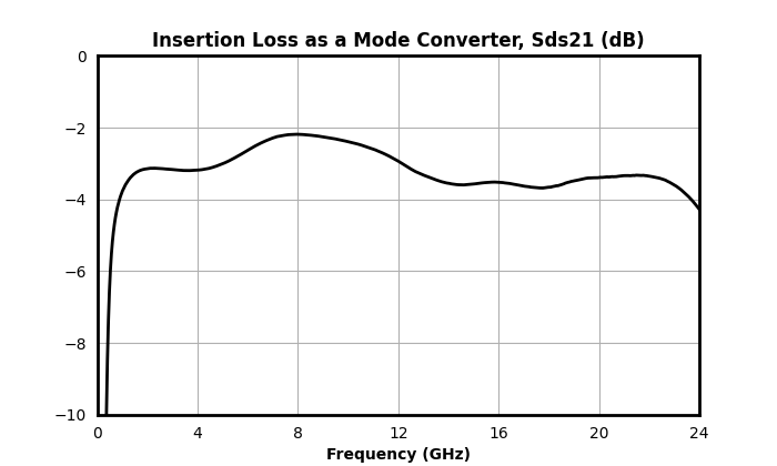
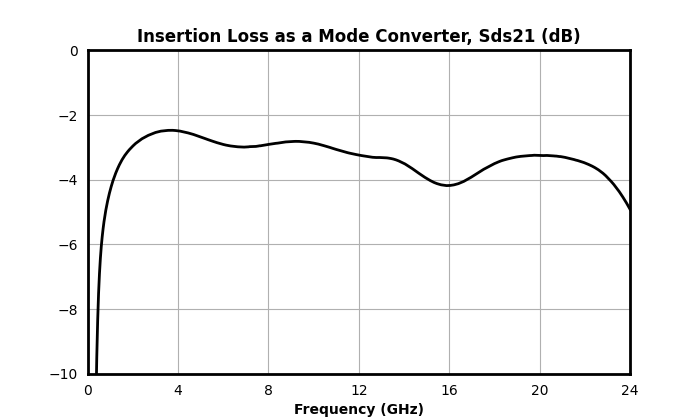
| Insertion Loss as a Mode Converter | 25°C | 0.5 | 20 | - | 3.6 | - | dB |
| Isolation | 25°C | 0.5 | 20 | - | 9 | - | dB |
| Nominal Phase Shift | 25°C | 0.5 | 20 | - | 180 | - | ° |
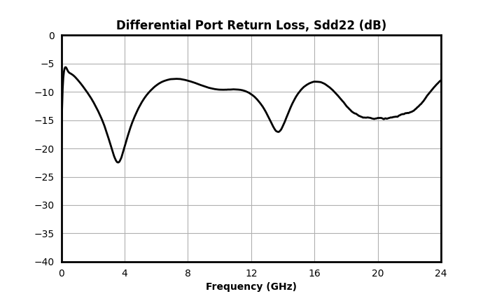
| Output Return Loss | 25°C | 0.5 | 20 | - | 7 | - | dB |
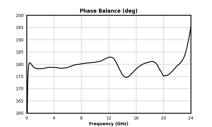
| Phase Balance | 25°C | 0.5 | 20 | - | 2 | - | ° |
| Impedance Ratio | - | - | - | - | 1:1 | - | - |
| Parameter | Test Conditions | Minimum Frequency (GHz) | Maximum Frequency (GHz) | Min | Typ | Max | Unit |
|---|---|---|---|---|---|---|---|
| Amplitude Balance | 25°C | 0.5 | 20 | - | 0.3 | - | dB |
| Common Mode Rejection | 25°C | 0.5 | 20 | - | 32 | - | dB |
| Common Port Return Loss | 25°C | 0.5 | 20 | - | 16 | - | dB |
| Impedance | 25°C | 0.5 | 20 | - | 50 | - | Ω |
| Insertion Loss as a Mode Converter | 25°C | 0.5 | 20 | - | 3.6 | - | dB |
| Isolation | 25°C | 0.5 | 20 | - | 9 | - | dB |
| Nominal Phase Shift | 25°C | 0.5 | 20 | - | 180 | - | ° |
| Output Return Loss | 25°C | 0.5 | 20 | - | 7 | - | dB |
| Phase Balance | 25°C | 0.5 | 20 | - | 2 | - | ° |
| Impedance Ratio | - | - | - | - | 1:1 | - | - |
MBALH-0R520CSP2
0.5-20 GHz Passive MMIC Chip Scale Package 1:1 Balun
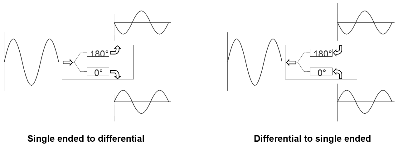
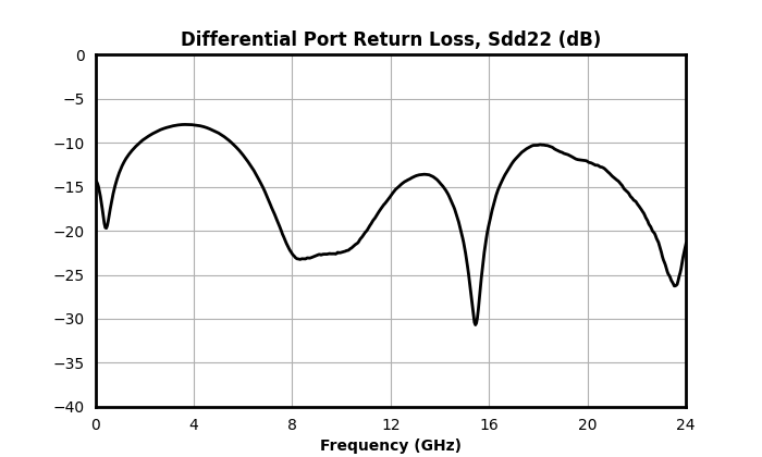
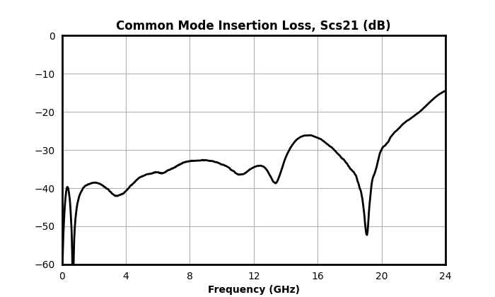
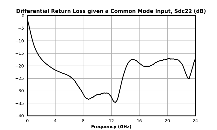
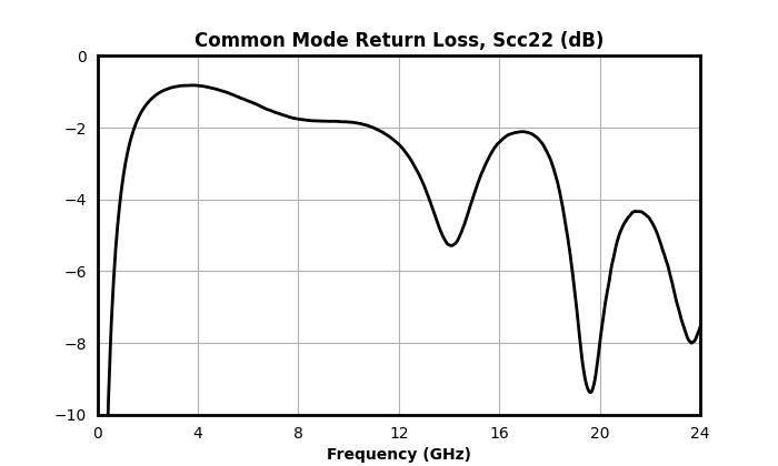
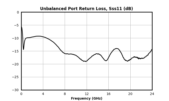
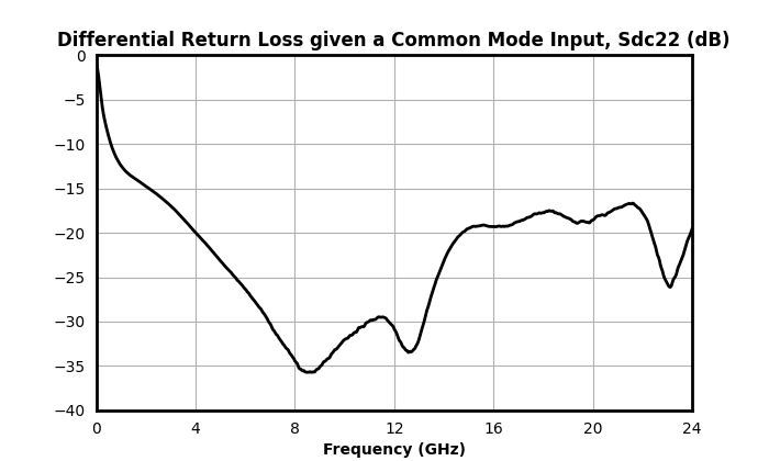
Mixed mode scattering parameters are used to characterize differential circuits. For baluns, this means that the 0° and 180° ports become a single 50Ω differential port and the common port remains the same 50Ω common port. For more information about 1:1 balun data, visitMBAL vs. MBALH Data. The two-port s-parameters of the balun are then characterized based on differential (d), common mode (c), or single-ended (s) signals. For example: Scs12 is the Common output response given a single ended input.
MBALH-0R520CSP2
0.5-20 GHz Passive MMIC Chip Scale Package 1:1 Balun

.png)


MBALH-0R520CSP2
0.5-20 GHz Passive MMIC Chip Scale Package 1:1 Balun

MBALH-0R520CSP2
0.5-20 GHz Passive MMIC Chip Scale Package 1:1 Balun
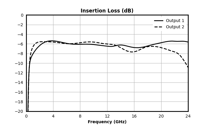
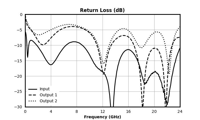


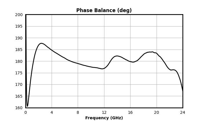
All measurements are de-embedded from the fixture with Automatic Fixture Removal (AFR).
MBALH-0R520CSP2
0.5-20 GHz Passive MMIC Chip Scale Package 1:1 Balun
Download : Outline 2D Drawing Outline 3D Drawing Outline 3D STP
-(0R106,%200R520)CSP2%20Catalog%20Outline-Model.png)
EVB Out- refers to output Out 1
EVB Out+ refers to output Out 2
MBALH-0R520CSP2
0.5-20 GHz Passive MMIC Chip Scale Package 1:1 Balun
Download : Footprint Drawing

MBALH-0R520CSP2
0.5-20 GHz Passive MMIC Chip Scale Package 1:1 Balun
| Parameter | Test Conditions | Frequency Range (GHz) | Min | Typ | Max | Unit |
|---|---|---|---|---|---|---|
| Impedance Ratio | - | - | - | 1 | - | - |
MBALH-0R520CSP2
0.5-20 GHz Passive MMIC Chip Scale Package 1:1 Balun
-(0R106,%200R520)%20Catalog%20Outline-Model.png)