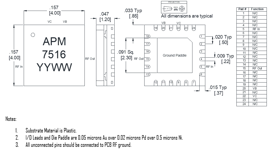
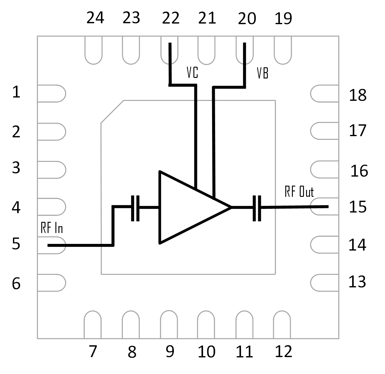
Port Diagram
A port diagram of the APM-7516PSM is shown below.
Sales: 408-778-9952 | General: 408-778-4200 | Fax: 408-778-4300
Sales & Customer Support: [email protected]
Tech Support: [email protected]
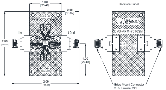
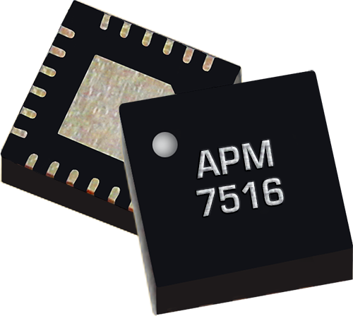
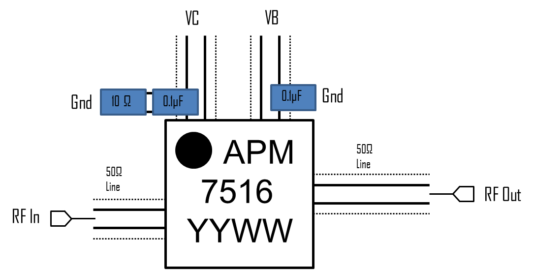
The APM-7516PSM is a broadband low phase noise driver amplifier designed to provide enough power to drive the LO port of an H or L-diode mixer with a range of input powers. This amplifier uses GaAs HBT technology for low phase noise and provides +18 to 23 dBm output power from 1.5 GHz to 20 GHz. This amplifier can be operated with a variety of bias conditions for both low and high-power applications. The APM-7516SM shows less variation in current supply under saturation than similar HBT amplifiers, has a lower thermal resistance, and is less sensitive to damage from high input powers. The APM-7516PSM is packaged in a compact 4 mm QFN with integrated blocking capacitors and power supply inductor for surface mount integration on circuit board-based systems.
| Part Number | Description | Package | Green Status | Product Lifecycle | Export Classification |
|---|---|---|---|---|---|
| APM-7516PSM | 1.5-20 GHz Surface Mount Low Phase Noise Amplifier | QFN | REACH RoHS | Released | EAR99 |
| EVB-APM-7516PSM | Evaluation Board, Low Phase Noise 1.5-20 GHz Amplifier | EVB | REACH RoHS | Released | EAR99 |
APM-7516PSM
1.5-20 GHz Surface Mount Low Phase Noise Amplifier
| Revision Code | Revision Date | Comment |
|---|---|---|
| - | 2022-01-01 | Datasheet Initial Release |
| A | 2026-02-13 | MTTF Table Added. |
APM-7516PSM
1.5-20 GHz Surface Mount Low Phase Noise Amplifier
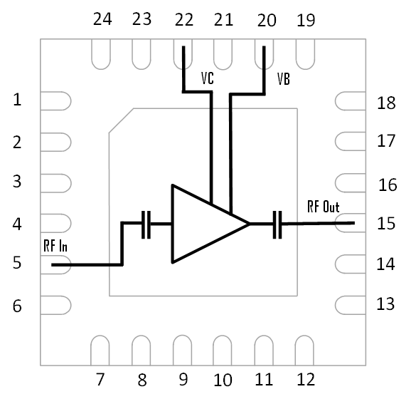
A port diagram of the APM-7516PSM is shown below.
| Port | Function | Description | DC Equivalent Circuit |
|---|---|---|---|
| 15 | RF Output Port | This is the amplifier’s RF Output. It is RF matched to 50 Ω and is DC blocked. Must have less than 7:1 VSWR when operating. |  |
| 20 | Current Mirror Bias Port | Port 20 is the DC voltage bias pad for the current mirror that controls the collector current supplied to the amplifier. See performance plot at different bias condition. |  |
| 22 | VC Power Supply Port | Pad VC is the amplifier’s DC voltage supply pad. See section performance plot at different bias conditions. |  |
| 5 | RF Input | This is the RF input port of the device, and is RF matched to 50 Ω. This port is AC-coupled; no blocking capacitor is required. |  |
| GND | Ground | IC backside must be connected to a DC/RF ground with high thermal and electrical conductivity. |  |
APM-7516PSM
1.5-20 GHz Surface Mount Low Phase Noise Amplifier
The Absolute Maximum Ratings indicate limits beyond which damage may occur to the device. If these limits are exceeded, the device may become inoperable or have a reduced lifetime.
| Parameter | Maximum Rating | Unit |
|---|---|---|
| Bias (Current Mirror) Voltage | 7 | V |
| Maximum Operating Temperature | 85 | °C |
| Maximum Storage Temperature | 150 | °C |
| Max Junction Temperature for MTTF > 1E6 Hours | 125 | °C |
| Max Power Dissipation for MTTF of 1E6 hours at 85˚C Baseplate Temperature | 1200 | mW |
| Minimum Operating Temperature | -40 | °C |
| Minimum Storage Temperature | -65 | °C |
| Output Load VSWR | 7 | - |
| Power Supply (Collector) Current (Ic) | 240 | mA |
| Power Supply (Collector) Voltage (VC) | 7 | V |
| RF Input Power | 18 | dBm |
| θJC, Junction to Case Thermal Resistance | 33 | ºC/W |
| T (°C) | λ (TIF) | MTTF (hr) | MTTF (yr) |
|---|---|---|---|
| 105 | 2,441.45 | 4.10E+05 | 47 |
| 85 | 310.48 | 3.22E+06 | 368 |
| 55 | 8.79 | 1.14E+08 | 12,992 |
| 25 | 0.12 | 8.24E+09 | 941,063 |
| Parameter | Details | Rating |
|---|---|---|
| Dimensions | - | 4 x 4 mm |
| Moisture Sensitivity Level | - | MSL 1 |
The Recommended Operating Conditions indicate the limits, inside which the device should be operated, to guarantee the performance given in Electrical Specifications Operating outside these limits may not necessarily cause damage to the device, but the performance may degrade outside the limits of the electrical specifications. For limits, above which damage may occur, see Absolute Maximum Ratings.
| Parameter | Min | Nominal | Max | Unit |
|---|---|---|---|---|
| Ambient Temperature | -40 | 25 | 85 | °C |
| Positive DC Voltage (VC) | 4 | 5 | 6 | V |
| Quiescent DC Current (Ic) | - | 105 | - | mA |
| DC Current with RF Input (Ic) | - | - | 225 | mA |
| Positive DC Current Mirror Voltage (VB) | - | 5 | - | V |
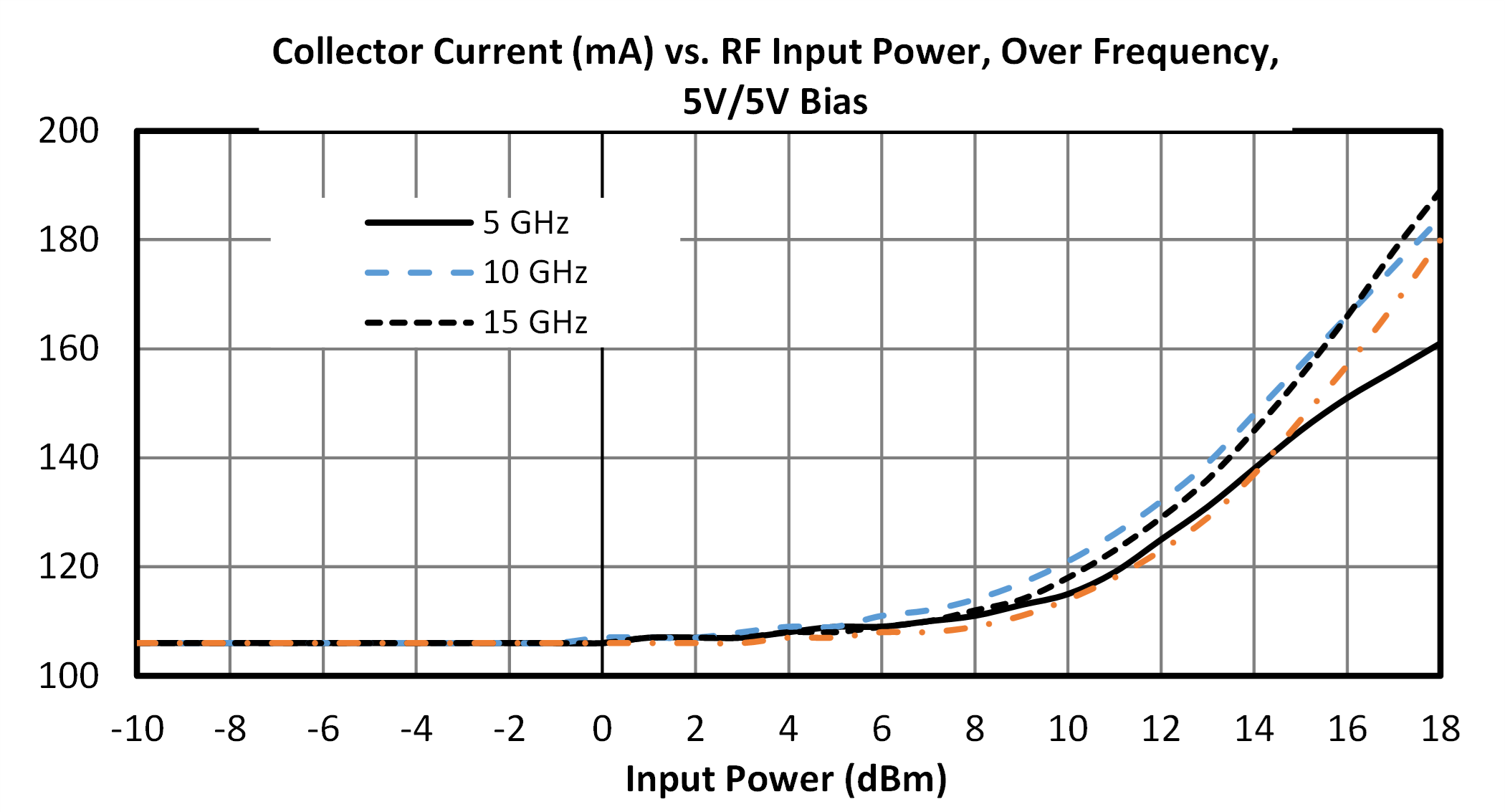
| Input Power for Saturation | 10 | 12 | 14 | dBm |
APM-7516PSM
1.5-20 GHz Surface Mount Low Phase Noise Amplifier
The electrical specifications apply at TA=+25 °C in a 50 Ω system. QFNs are 100% RF tested.
| Parameter | Test Conditions | Minimum Frequency (GHz) | Maximum Frequency (GHz) | Min | Typ | Max | Unit |
|---|---|---|---|---|---|---|---|
| Input IP3 | Power Supply Voltage Vc = 5V Bias Voltage Vb = 5V -5 dBm Input power | 1.5 | 20 | - | 21 | - | dBm |
| Input Power for Saturation | Power Supply Voltage Vc = 5V Bias Voltage Vb = 5V | 1.5 | 20 | - | 12 | - | dBm |
| Input Return Loss | Power Supply Voltage Vc = 5V Bias Voltage Vb = 5V | 1.5 | 20 | - | 16 | - | dB |
| Noise Figure | - | 15 | 20 | - | 6.5 | - | dB |
| Noise Figure | - | 1.5 | 5 | - | 9.7 | - | dB |
| Noise Figure | - | 5 | 15 | - | 5.4 | - | dB |
| Output IP3 | Power Supply Voltage Vc = 5V Bias Voltage Vb = 5V -5 dBm Input power | 1.5 | 20 | - | 33 | - | dBm |
| Output Return Loss | Power Supply Voltage Vc = 5V Bias Voltage Vb = 5V | 1.5 | 20 | - | 17 | - | dB |
| Power Dissipated as a Linear Signal Amplifier 1 | Power Supply Voltage Vc = 5V Bias Voltage Vb = 5V | 1.5 | 20 | - | 525 | - | mW |
| Power Dissipated as a Saturated LO Driver Amplifier 2 | Power Supply Voltage Vc = 5V Bias Voltage Vb = 5V | 1.5 | 20 | - | 650 | - | mW |
| Reverse Isolation | Power Supply Voltage Vc = 5V Bias Voltage Vb = 5V | 1.5 | 20 | - | 34 | - | dB |
| Saturated Output Power | Power Supply Voltage Vc = 5V, Bias Voltage Vb = 5V, P5dB | 1.5 | 20 | - | 22 | - | dBm |
| Small Signal Gain | Power Supply Voltage Vc = 5V Bias Voltage Vb = 5V | 1.5 | 20 | - | 11 | - | dB |
[1][2] Power dissipated = DC input power + RF input power – RF output power. Linear signal amplifier operation is with quiescent current and low output power. Saturated LO Driver calculated with recommended input power for saturation.
APM-7516PSM
1.5-20 GHz Surface Mount Low Phase Noise Amplifier
APM-7516PSM measurements taken in EVAL-APM-7516PSM evaluation board without de-embedding.


APM-7516PSM
1.5-20 GHz Surface Mount Low Phase Noise Amplifier


APM-7516PSM
1.5-20 GHz Surface Mount Low Phase Noise Amplifier


APM-7516PSM
1.5-20 GHz Surface Mount Low Phase Noise Amplifier
APM-7516PSM
1.5-20 GHz Surface Mount Low Phase Noise Amplifier
APM-7516PSM
1.5-20 GHz Surface Mount Low Phase Noise Amplifier
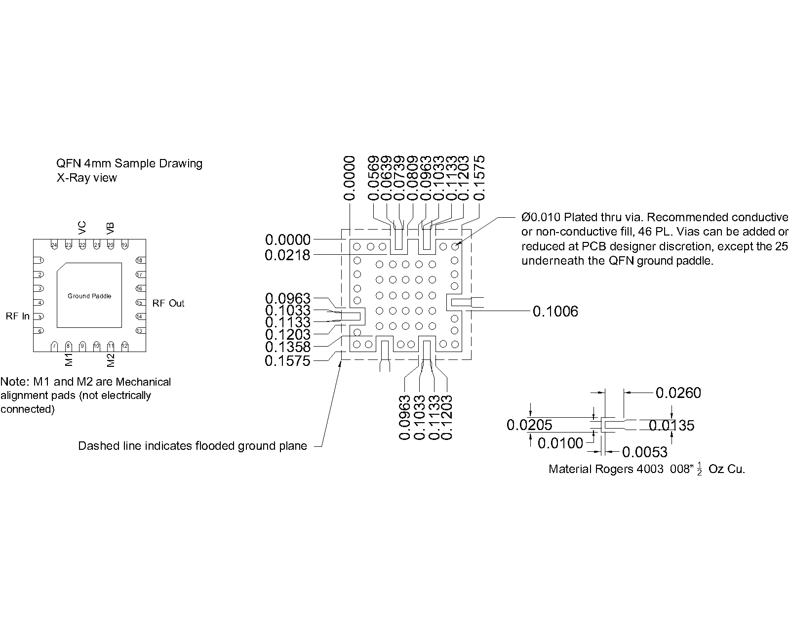
Download : Footprint Drawing
APM-7516PSM
1.5-20 GHz Surface Mount Low Phase Noise Amplifier