Port Diagram
A top-down (left) and bottom-up (right) view of the AMM-6702SM’s KFN package outline drawing is shown below. The pin functions are detailed in this datasheet.

NOT RECOMMENDED FOR NEW DESIGN
Sales: 408-778-9952 | General: 408-778-4200 | Fax: 408-778-4300
Sales & Customer Support: [email protected]
Tech Support: [email protected]
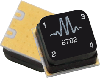
The AMM-6702SM is a surface-mount LO driver amplifier that is designed to provide sufficient LO drive for an H or S diode mixer such as the MM1-1850HSM or MM1-1850SSM across temperature with input power from 0-10 dBm. This ferritic package offers improved resilience to radiative feedback and oscillatory behavior over the bare-die package option, providing the customer with a compact, high gain, wideband LO driver amplifier.

| Part Number | Description | Package | Green Status | Product Lifecycle | Export Classification | Recommended Replacement |
|---|---|---|---|---|---|---|
| AMM-6702SM | 20-50 GHz GaAs Surface Mount LO Driver Amplifier | KFN | REACH RoHS | Not Recommended for New Design | 3A001.b.2.d | AMM-10202PSM |
| EVAL-AMM-6702SM | Evaluation Board, 20-50 GHz GaAs Surface Mount LO Driver Amplifier | EVAL | REACH RoHS | Not Recommended for New Design | EAR99 | EVB-AMM-10202P |
AMM-6702SM
20-50 GHz GaAs Surface Mount LO Driver Amplifier
| Revision Code | Revision Date | Comment |
|---|---|---|
| - | 2019-10-01 | Datasheet Initial Release |
| A | 2019-10-01 | Updated Performance Plots |
| B | 2019-11-01 | Mixer Performance Plots & Application Circuits |
| C | 2019-11-01 | Production fixture minimum gain spec modified |
| D | 2020-01-01 | Gain and Power Output Performance Plots Updated |
| E | 2020-02-01 | Added content |
| F | 2020-06-01 | Updated Maximum Ratings |
| G | 2020-08-01 | Updated Landing Pattern |
| H | 2020-11-01 | Updated Thermal Specs and IP3 specs, added link to landing pattern |
| I | 2020-11-01 | Updated Min Frequency Spec |
| J | 2023-11-07 | Updated thermal resistance and maximum power dissipation, indicating typical operation. |
| K | 2024-07-26 | Reduced Recommended Supply Voltage to 3V |
| L | 2026-02-13 | MTTF Table Added. |
AMM-6702SM
20-50 GHz GaAs Surface Mount LO Driver Amplifier
A top-down (left) and bottom-up (right) view of the AMM-6702SM’s KFN package outline drawing is shown below. The pin functions are detailed in this datasheet.
| Port | Function | Description | DC Equivalent Circuit |
|---|---|---|---|
| GND | Ground | Bottom side must be connected to a DC/RF ground potential with high thermal and electrical conductivity. |  |
| Pin 1 | Positive DC Supply Vd | Pin 1 provides +2V to +4V DC voltage and drain current to the amplifier. Negative voltage must be supplied to Pin 4 before turning on the positive supply voltage. |  |
| Pin 2 | RF Input | Pin 2 is the RF input of the amplifier. It is internally DC blocked. |  |
| Pin 3 | RF Output | Pin 3 is the RF output of the amplifier. It is internally DC blocked. | |
| Pin 4 | Negative DC Supply Vg | Pin 4 provides -0.4V to -0.6V of DC voltage. This must be turned on before turning on the positive supply voltage to Pin 1. |  |
AMM-6702SM
20-50 GHz GaAs Surface Mount LO Driver Amplifier
The Absolute Maximum Ratings indicate limits beyond which damage may occur to the device. If these limits are exceeded, the device may be inoperable or have a reduced lifetime.
| Parameter | Maximum Rating | Unit |
|---|---|---|
| Continuous Power Dissipation (PDISS) | 1.2 | W |
| Maximum Operating Temperature | 85 | °C |
| Maximum Storage Temperature | 150 | °C |
| Max Junction Temperature for MTTF > 1E6 Hours | 175 | °C |
| Minimum Operating Temperature | -40 | °C |
| Minimum Storage Temperature | -65 | °C |
| Negative Bias Current (Pin 4) | 10 | μA |
| Negative Bias Voltage (Pin4) | -2 | V |
| Positive Bias Current (Pin1) 1 | 400 | mA |
| Positive Bias Voltage (Pin1) | 4.5 | V |
| RF Input Power | 22 | dBm |
| Thermal Resistance, θJC | 78.5 | ºC/W |
Maximum Continuous Power Dissipation indicates power that will maintain an MTTF > 1E6 hours under typical operating conditions at max operating temperature. Specific use cases may differ, contact support for more detailed information.
[1] Maximum current draw is 400 mA when not limited by continuous power dissipation rating
| T (°C) | λ (TIF) | MTTF (hr) | MTTF (yr) |
|---|---|---|---|
| 105 | 2,441.45 | 4.10E+05 | 47 |
| 85 | 310.48 | 3.22E+06 | 368 |
| 55 | 8.79 | 1.14E+08 | 12,992 |
| 25 | 0.12 | 8.24E+09 | 941,063 |
| Parameter | Details | Rating |
|---|---|---|
| ESD | < 250 Volts | HBM Class 0 |
| Dimensions | - | 4 x 4 mm |
| Moisture Sensitivity Level | - | MSL 1 |
The Recommended Operating Conditions indicate the limits, inside which the device should be operated, to guarantee the performance given in Electrical Specifications. Operating outside these limits may not necessarily cause damage to the device, but the performance may degrade outside the limits of the Electrical Specifications. For limits, above which damage may occur, see Absolute Maximum Ratings.
| Parameter | Min | Nominal | Max | Unit |
|---|---|---|---|---|
| Ambient Temperature | -55 | 25 | 85 | °C |
| Positive DC Current | 100 | 180 | 350 | mA |
| Negative DC Voltage | -0.4 | -0.5 | -0.6 | V |
| Positive DC Voltage | 2 | 3 | 3 | V |
AMM-6702SM
20-50 GHz GaAs Surface Mount LO Driver Amplifier
The electrical specifications apply at TA=+25°C in a 50Ω system. Min and Max limits apply only to our connectorized units and are guaranteed at TA=+25°C. Minimum test specifications are verified up to 44 GHz within an EVAL fixture due to the high insertion loss of the fixture above 45 GHz.
| Parameter | Test Conditions | Minimum Frequency (GHz) | Maximum Frequency (GHz) | Min | Typ | Max | Unit |
|---|---|---|---|---|---|---|---|
| Current Consumption 1 | 3V/-0.4V | 21 | 50 | - | 230 | - | mA |
| Current Consumption 2 | 3V/-0.5V | 21 | 50 | - | 180 | - | mA |
| Current Consumption 3 | 3V/-0.6V | 21 | 50 | - | 130 | - | mA |
| Input IP3 | 3V/-0.5V bias, -25 dBm Input Power | 21 | 50 | - | 3 | - | dBm |
| Input Return Loss | 3V/-0.5V bias, -25 dBm Input Power | 21 | 50 | - | 8 | - | dB |
| Noise Figure | 3V/-0.5V bias, -25 dBm Input Power | 21 | 50 | - | 6.5 | - | dB |
| Output IP3 | 3V/-0.5V bias, -25 dBm Input Power | 21 | 50 | - | 27 | - | dBm |
| Output P1dB | 3V/-0.5V bias | 21 | 50 | - | 14.8 | - | dBm |
| Output Return Loss | 3V/-0.5V bias, -25 dBm Input Power | 21 | 50 | - | 9 | - | dB |
| Reverse Isolation | 3V/-0.5V bias, -25 dBm Input Power | 21 | 50 | - | 45 | - | dB |
| Saturated Output Power | 3V/-0.5V bias, +5 dBm Input Power | 21 | 50 | - | 19 | - | dBm |
| Small Signal Gain | 3V/-0.5V bias, -25 dBm Input Power | 21 | 50 | - | 24 | - | dB |
[1][2][3] Bias conditions tested with no RF input power. See Typical Performance Plots for DC current vs. RF power
AMM-6702SM
20-50 GHz GaAs Surface Mount LO Driver Amplifier
Measurement data extracted from within the EVAL-AMM-6702SM module. Insertion loss of the EVAL board has been extracted from the small signal gain and output power measurements.
⁶ Temperature-controlled output power measurements were performed in the EVAL-AMM-6702SM test fixture with 3V/-0.5V bias and +10 dBm RF input power


AMM-6702SM
20-50 GHz GaAs Surface Mount LO Driver Amplifier


AMM-6702SM
20-50 GHz GaAs Surface Mount LO Driver Amplifier
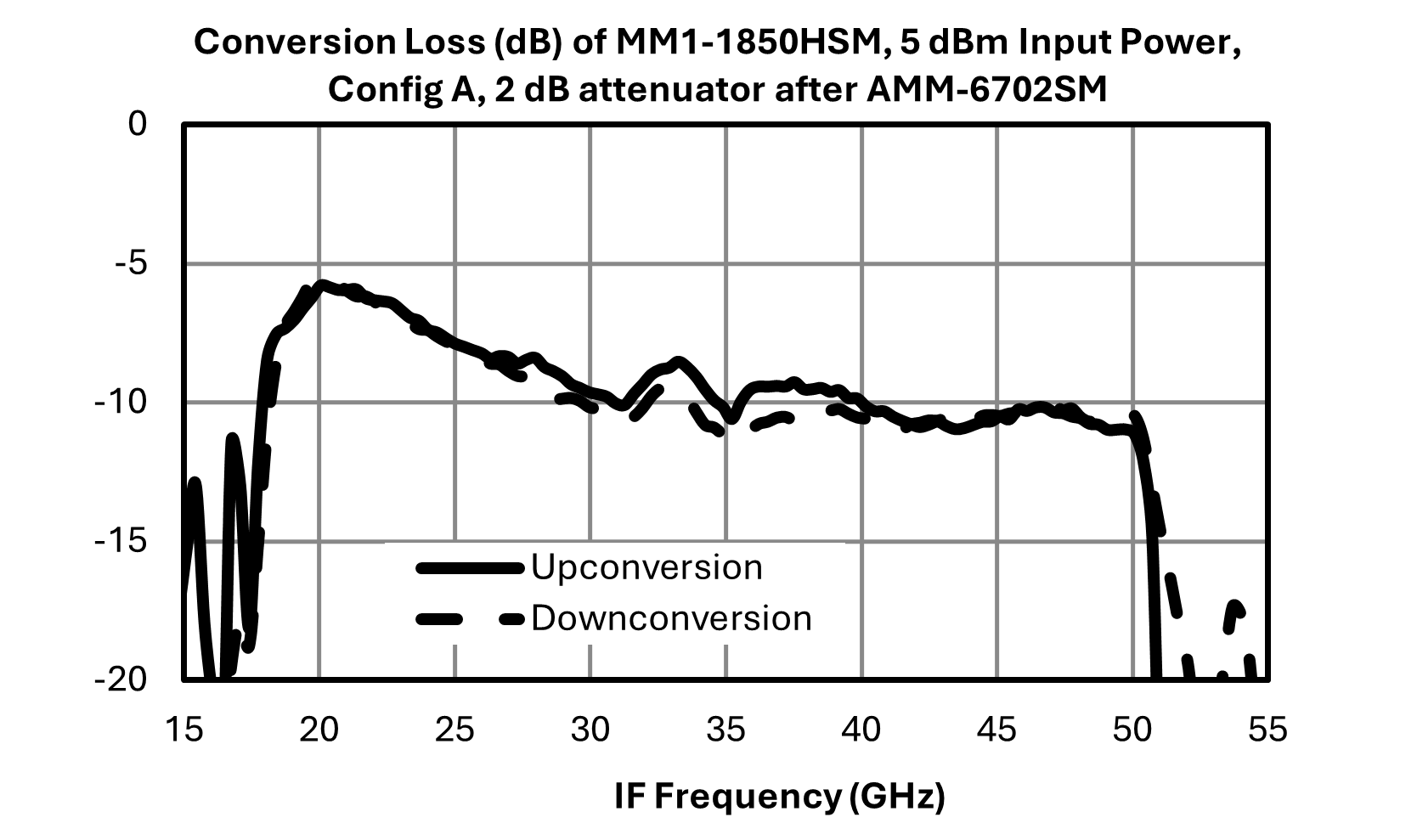
Conversion loss plots taken using custom AMM-6702SM/MM1-1850SM connectorized EVAL board. RF path insertion loss is ~1.5 dB at 50 GHz.

AMM-6702SM
20-50 GHz GaAs Surface Mount LO Driver Amplifier
AMM-6702SM
20-50 GHz GaAs Surface Mount LO Driver Amplifier
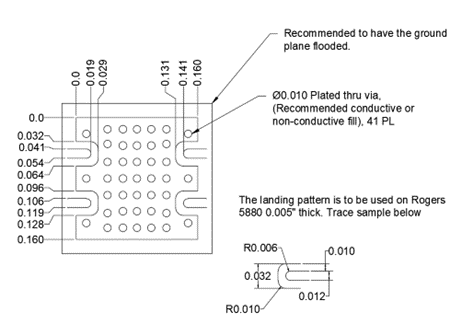
Download : Footprint Drawing
AMM-6702SM
20-50 GHz GaAs Surface Mount LO Driver Amplifier

