Port Diagram

Sales: 408-778-9952 | General: 408-778-4200 | Fax: 408-778-4300
Sales & Customer Support: [email protected]
Tech Support: [email protected]
The ADM-8622PSM is a high-linearity low noise amplifier capable of providing 15.5 dB gain, 2 dB noise figure and +26 dBm OIP3 up to 10 GHz. The amplifier is suitable for use in RF front-ends requiring low noise, high gain and excellent signal fidelity. The ADM-8622PSM performs well down to DC and its low frequency performance is limited only by the frequency response of the input and output bias tees present in the application circuit. The ADM-8622PSM is available in a very compact 1.3x2mm DFN package.


| Part Number | Description | Package | Green Status | Product Lifecycle | Export Classification |
|---|---|---|---|---|---|
| ADM-8622PSM | DC - 10 GHz High Dynamic Range Gain Block | DFN | REACH RoHS | Released | EAR99 |
| EVB-ADM-8622P | Evaluation Board, DC - 10 GHz High Dynamic Range Gain Block Amplifier | EVB | REACH RoHS | Released | EAR99 |
ADM-8622PSM
DC - 10 GHz High Dynamic Range Gain Block
| Revision Code | Revision Date | Comment |
|---|---|---|
| - | 2023-06-01 | Initial Datasheet Release |
| A | 2025-03-04 | Corrected Application Circuit Voltage |
| B | 2025-05-07 | Updated Abs Max Drain Voltage from 4V to 7V |
ADM-8622PSM
DC - 10 GHz High Dynamic Range Gain Block
ADM-8622PSM
DC - 10 GHz High Dynamic Range Gain Block
| Port | Function | Description | DC Equivalent Circuit |
|---|---|---|---|
| Paddle | Gnd | Package ground paddle must be connected to a DC/RF ground potential with high thermal and electrical conductivity. | - |
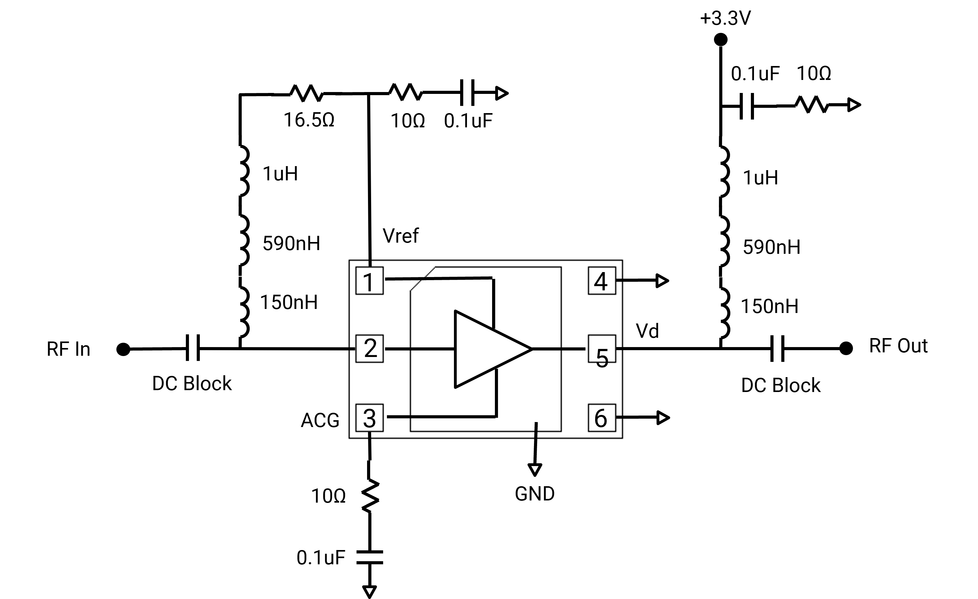
| Pin 1 | Vref | Pin 1 provides a voltage reference to bias Pin 2. Pin 1 and pin 2 must be DC coupled but RF isolated by a choke. For proper operation, DO NOT ground this pin nor leave it floating . See application section for more details. | - |
| Pin 2 | RF Input | Pin 2 is the RF Input port of the amplifier. It is internally RF matched to 50 Ω and requires an external DC blocking cap. Pin 2 must be DC coupled to Pin 1 voltage reference through an RF choke for biasing. | - |
| Pin 3 | ACG | Pin 3 should be AC grounded using a series RC network. See application section for details. DO NOT DC GROUND THIS PIN. | - |
| Pin 4,6 | NC | Pin 4 and Pin 6 are internally no-connects and should be connected to DC/RF ground. | - |
| Pin 5 | RF Out / Vd | Pin 5 is the RF Output port and is also the Vd port providing the main power supply to the amplifier. This pin is DC coupled and requires an external bias-T or discrete choke and DC blocking capacitor. This port is RF matched to 50 Ω. DC voltage at this pin should be set to 3.3V for normal operation. | - |
ADM-8622PSM
DC - 10 GHz High Dynamic Range Gain Block
The Absolute Maximum Ratings indicate limits beyond which damage may occur to the device. If any one of these limits are exceeded, the device may become inoperable or have a reduced lifetime. Reliability limits are individual, instantaneous catastrophic limits only. Functional operation limits are indicated below. Operation of the device at multiple absolute maximum limits or for extended periods at a single limit can cause degradation and damage to the device.
| Parameter | Maximum Rating | Unit |
|---|---|---|
| Drain Bias Current (Idq) | 60 | mA |
| Drain Supply Voltage (Vd) | 7 | V |
| Maximum Operating Temperature for MTTF > 1E6 hours | 85 | °C |
| Maximum Storage Temperature | 125 | °C |
| Max Junction Temperature for MTTF of >1E6 hours | 175 | °C |
| Max Power Dissipation for MTTF of > 1E6 hours | 0.72 | W |
| Minimum Operating Temperature for MTTF > 1E6 hours | -40 | °C |
| Minimum Storage Temperature | -65 | °C |
| Reference Bias Current (Iref) | 15 | mA |
| Reference Bias Voltage (Vref) | 2 | V |
| RF Input Power | 20 | dBm |
| θ_Jc, Junction to Case Thermal Resistance | 50 | ºC/W |
| Parameter | Details | Rating |
|---|---|---|
| Weight | Package name: DFN | 0.007g |
| Dimensions | - | 2.0 x 1.3 mm |
| Moisture Sensitivity Level | - | MSL 1 |
The Recommended Operating Conditions indicate the limits, inside which the device should be operated, to guarantee the performance given in Electrical Specifications Operating outside these limits may not necessarily cause damage to the device, but the performance may degrade outside the limits of the electrical specifications. For limits, above which damage may occur, see Absolute Maximum Ratings.
| Parameter | Min | Nominal | Max | Unit |
|---|---|---|---|---|
| Ta Ambient Temperature | -40 | 25 | 85 | °C |
| Power Supply DC Voltage (Vd) | - | 3.3 | - | V |
| Power Supply DC Current (Idq) (No RF Input) | - | 40 | - | mA |
| Input Power for Saturation | - | 5 | - | dBm |
ADM-8622PSM
DC - 10 GHz High Dynamic Range Gain Block
Unless otherwise specified, electrical specifications apply at TA=+25°C and Vd = 3.3 V.
| Parameter | Test Conditions | Minimum Frequency (GHz) | Maximum Frequency (GHz) | Min | Typ | Max | Unit |
|---|---|---|---|---|---|---|---|
| Current Consumption | Vd = 3.3 V no RF input | - | - | - | 40 | - | mA |
| Input IP2 | Vd = 3.3 V Idq = 40mA Pin = -18 dBm per tone, 1 MHz tone spacing | 0 | 10 | - | 14 | - | dBm |
| Input IP3 | Vd = 3.3 V Idq = 40mA Pin = -18 dBm per tone, 1 MHz tone spacing | 0 | 10 | - | 11 | - | dBm |
| Input Power for Saturation | Vd = 3.3 V Idq = 40mA | 0 | 10 | - | 5 | - | dBm |
| Input Return Loss | Vd = 3.3 V Idq = 40mA Pin = -20 dBm | 0 | 10 | - | 16 | - | dB |
| Noise Figure | Vd = 3.3 V Idq = 40mA Pin = -20 dBm | 0.21 | 10 | - | 2 | - | dB |
| Output IP2 | Vd = 3.3 V Idq = 40mA Pin = -18 dBm per tone, 1 MHz tone spacing | 0 | 10 | - | 29 | - | dBm |
| Output IP3 | Vd = 3.3 V Idq = 40mA Pin = -18 dBm per tone, 1 MHz tone spacing | 0 | 10 | - | 26 | - | dBm |
| Output P1dB | Vd = 3.3 V Idq = 40mA | 0 | 10 | - | 13.5 | - | dBm |
| Output Return Loss | Vd = 3.3 V Idq = 40mA Pin = -20 dBm | 0 | 10 | - | 24 | - | dB |
| Reverse Isolation | Vd = 3.3 V Idq = 40mA Pin = -20 dBm | 0 | 10 | - | 19 | - | dB |
| Saturated Output Power | Vd = 3.3 V Idq = 40mA | 0 | 10 | - | 15 | - | dBm |
| Small Signal Gain | Vd = 3.3 V Idq = 40mA Pin = -20 dBm | 0 | 10 | - | 15.5 | - | dB |
ADM-8622PSM
DC - 10 GHz High Dynamic Range Gain Block


ADM-8622PSM
DC - 10 GHz High Dynamic Range Gain Block


ADM-8622PSM
DC - 10 GHz High Dynamic Range Gain Block
ADM-8622PSM
DC - 10 GHz High Dynamic Range Gain Block
ADM-8622PSM
DC - 10 GHz High Dynamic Range Gain Block
Download : Footprint Drawing

ADM-8622PSM
DC - 10 GHz High Dynamic Range Gain Block


ADM-8622PSM
DC - 10 GHz High Dynamic Range Gain Block


ADM-8622PSM
DC - 10 GHz High Dynamic Range Gain Block

