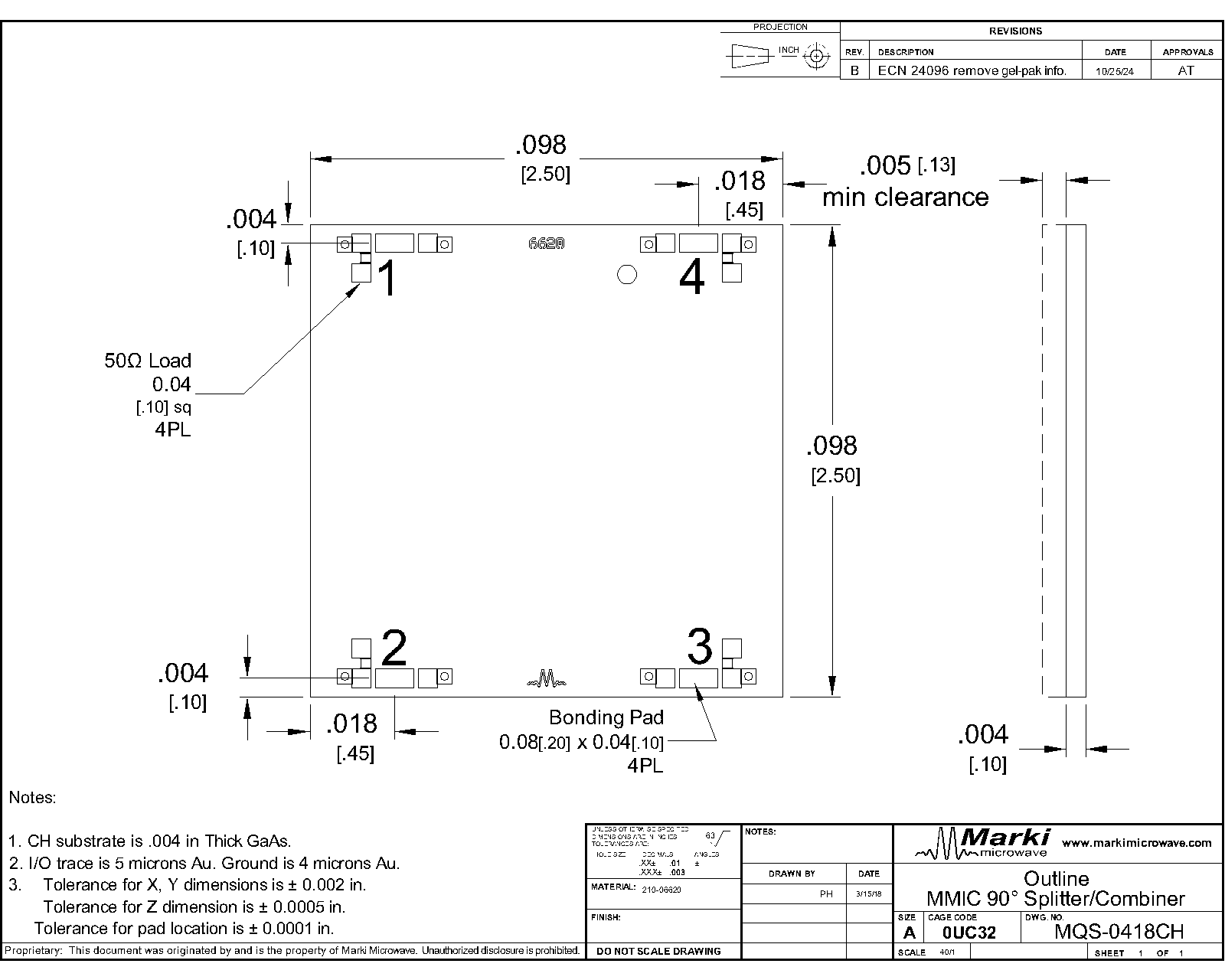
Device Overview

General Description

The MQS-0418 is a MMIC 4GHz – 18GHz 90° splitter/combiner. Wire bondable 50Ω terminations are available on-chip. Passive GaAs MMIC technology allows production of smaller constructions that replace larger form factor circuit board constructions. Tight fabrication tolerances allow for less unit to unit variation than traditional splitter/combiner technologies. The MQS-0418 is available as a wire bondable chip and connectorized module. Low variation allows for accurate simulations using the provided S4P file taken from measured production units. The MQS-0418 is not recommended for applications involving reflected signals.

Photo of MQS-0418CH

Features

  • Designed for C to Ku-band applications
  • High amplitude and phase balance
  • High isolation
  • Low insertion loss
  • On-chip 50Ω load terminations

Applications

  • Single Sideband Upconverters
  • Image Rejection Downconverters
  • IQ Modulators
  • Balanced Amplifiers
  • Microwave Correlators

Functional Block Diagram

Block Diagram

Part Ordering Options

Part NumberDescriptionPackageConnectorsGreen StatusProduct LifecycleExport Classification
MQS-0418UAMMIC 4-18GHz 90° Splitter / CombinerUAStandard

REACH

RoHS

ReleasedEAR99
MQS-0418CHMMIC 4-18GHz 90° Splitter / CombinerCH-

REACH

RoHS

ReleasedEAR99

Table Of Contents

Revision History

Revision CodeRevision DateComment
-2018-08-01Datasheet Initial Release

Rev: - | Copyright © 2018 Marki Microwave LLC.

2

Port Configuration and Functions

Port Diagram

A top-down view of the MQS-0418CH package outline drawing is shown below. Only ports 1 and 2 may be used as an input. Ports 3 and 4 are not recommended as inputs. Device is not recommended for applications requiring reflected signals. Ports 1 – 4 correspond to the UA package designation.

Diagram of the port configuration for MQS-0418CH

Port Functions

Configuration A

PortFunctionDescriptionDC Equivalent
Circuit
PadGround CH package ground path is provided through the substrate and ground bond pads.Equivalent circuit for the Ground
Port 1Input Port 1 is DC short to port 3 and open to ground.Equivalent circuit for the Input
Port 290° Output Port 2 is DC short to port 4 and open to ground.Equivalent circuit for the 90° Output
Port 30° Output Port 3 is DC short to port 1 and open to ground.Equivalent circuit for the 0° Output
Port 4Isolated Port 4 is DC short to port 2 and open to ground.Equivalent circuit for the Isolated

Rev: - | Copyright © 2018 Marki Microwave LLC.

3

Configuration B

PortFunctionDescriptionDC Equivalent
Circuit
PadGround CH package ground path is provided through the substrate and ground bond pads.Equivalent circuit for the Ground
Port 190° Output Port 1 is DC short to port 3 and open to ground.Equivalent circuit for the 90° Output
Port 2Input Port 2 is DC short to port 4 and open to ground.Equivalent circuit for the Input
Port 3Isolated Port 3 is DC short to port 1 and open to ground.Equivalent circuit for the Isolated
Port 40° Output Port 4 is DC short to port 2 and open to ground.Equivalent circuit for the 0° Output

Rev: - | Copyright © 2018 Marki Microwave LLC.

4

Specifications

Absolute Maximum Ratings

The Absolute Maximum Ratings indicate limits beyond which damage may occur to the device. If these limits are exceeded, the device may be inoperable or have a reduced lifetime.

ParameterMaximum RatingUnit
Maximum Storage Temperature 125°C
Minimum Operating Temperature 100°C
Minimum Operating Temperature -55°C
Minimum Storage Temperature -65°C

Package Information

ParameterDetailsRating
Dimensions-2.50 x 2.50 mm

Rev: - | Copyright © 2018 Marki Microwave LLC.

5

Electrical Specifications

The electrical specifications apply at TA=+25°C in a 50Ω system. Min and Max limits are guaranteed at TA=+25°C. Device is non-reciprocal. Operation not guaranteed when ports 3 or 4 are used as an input.

ParameterPort ConfigurationTest ConditionsMinimum
Frequency
(GHz)
Maximum
Frequency
(GHz)
MinTypMaxUnit
Amplitude Balance --4 18-0.42dB
Excess Insertion Loss --4 18-1.53.2dB
Impedance --4 18-50-Ω
Isolation --4 181116-dB
Mean Coupling --4 18-3-dB
Nominal Phase Shift --4 18-90-°
Phase Balance --4 18-0.58°
VSWR --4 18-1.1-

Rev: - | Copyright © 2018 Marki Microwave LLC.

6

Typical Performance Plots

All measurements taken in a 50Ω environment. On-chip load was not used when taking measurements.

Bare Die Insertion Loss, Port 1 Input (dB) graph for MQS-0418CH
Bare Die Insertion Loss, Port 2 Input (dB) graph for MQS-0418CH
Bare Die Amplitude Balance, Port 1 Input (dB) graph for MQS-0418CH
Bare Die Amplitude Balance, Port 2 Input (dB) graph for MQS-0418CH
Bare Die Phase Balance, Port 1 Input (dB) graph for MQS-0418CH
Bare Die Amplitude Balance, Port 2 Input (dB) graph for MQS-0418CH

Rev: - | Copyright © 2018 Marki Microwave LLC.

7

Bare Die Return Loss (dB) graph for MQS-0418CH
Bare Die Isolation (dB) graph for MQS-0418CH

Rev: - | Copyright © 2018 Marki Microwave LLC.

8

MQS-0418UA - Typical Performance Plots

Phase balance spread is shown due to large performance spread. Minimal variance observed in amplitude balance and insertion loss. Performance spread is related to packaging and bond wire inductance variation.

Performance plots for the connectorized module are shown for measurements where directly probed measurements of the die are unavailable. Note that the following measurements include losses from connectors and microstrip traces.

Connectorized Module Insertion Loss, Port 1 Input (dB) graph for MQS-0418UA
Connectorized Module Insertion Loss, Port 2 Input (dB) graph for MQS-0418UA
Connectorized Module Amplitude Balance, Port 1 Input (dB) graph for MQS-0418UA
Connectorized Module Amplitude Balance, Port 2 Input (dB) graph for MQS-0418UA
Connectorized Module Phase Balance, Port 1 Input (dB) graph for MQS-0418UA
Connectorized Module Phase Balance, Port 2 Input (dB) graph for MQS-0418UA

Rev: - | Copyright © 2018 Marki Microwave LLC.

9

Connectorized Module Phase Balance, Port 1, Five Unit Spread (dB) graph for MQS-0418UA
Connectorized Module Phase Balance, Port 2, Five Unit Spread (dB) graph for MQS-0418UA
Connectorized Module Return Loss (dB) graph for MQS-0418UA
Connectorized Module Isolation (dB) graph for MQS-0418UA

Rev: - | Copyright © 2018 Marki Microwave LLC.

10

Mechanical Data

Outline Drawing

Download : Outline 2D Drawing

Outline Drawing

Rev: - | Copyright © 2018 Marki Microwave LLC.

11