Rev: B | Copyright © 2017, 2019 Marki Microwave LLC.

General Description

NLTL-6273SM is a MMIC non-linear transmission line (NLTL) based comb generator. This NLTL offers excellent phase noise performance over a low 0.7 to 5 GHz input frequency range with output tones to 24 GHz. NLTL-6273SM is fabricated with GaAs Schottky diode based varactors and packaged into a surface mount 5x5 mm2 QFN.

Features

  • Low Phase Noise
  • Broadband Input Frequencies
  • No External DC Bias Required

Functional Block Diagram

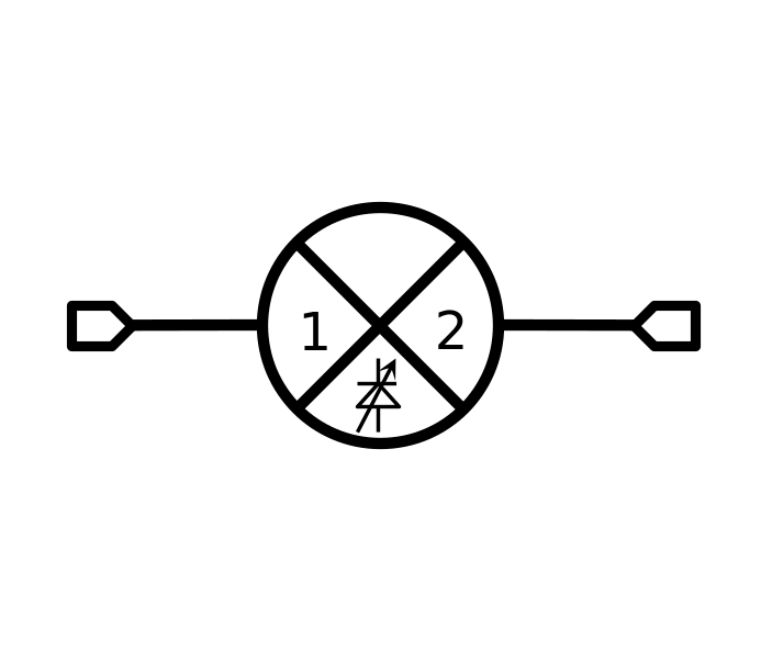
Block Diagram
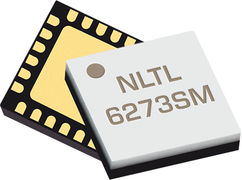
Photo of NLTL-6273SM

Electrical Performance Summary

ParameterTypUnit
Input Power 16 to 26dBm
Output Frequency Range 0.7 to 24GHz
Input Frequency Range 0.7 to 5GHz

Summary only – refer to the Electrical Specifications, Absolute Maximum Ratings, and Recommended Operating Range tables for complete details.

Part Ordering Options

Part NumberDescriptionPackagePacking SizeGreen StatusProduct LifecycleExport Classification
NLTL-6273SMGaAs MMIC Non-Linear Transmission LineQFN-

RoHS

REACH

ReleasedEAR99
EVAL-NLTL-6273Evaluation Board, GaAs MMIC 0.7-5 GHz Non-Linear Transmission LineEVAL-

RoHS

REACH

ReleasedEAR99
NLTL-6273-TRTape and Reel, GaAs MMIC Non-Linear Transmission LineQFN13"

RoHS

REACH

ReleasedEAR99

Table Of Contents

Typical Performance Plots

Typical Performance Plots

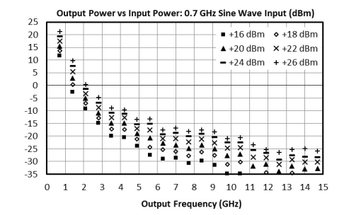
Output Power vs Input Power: 7 GHz Sine Wave Input (dBm) graph for NLTL-6273SM
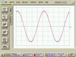
0.7 GHz +24 dBm Sine Wave Input graph for NLTL-6273SM
NLTL Output for 0.7 GHz +24 dBm Sine Wave Input graph for NLTL-6273SM
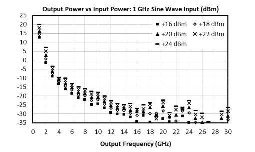
Output Power vs Input Power: 1 GHz Sine Wave Input (dBm) graph for NLTL-6273SM
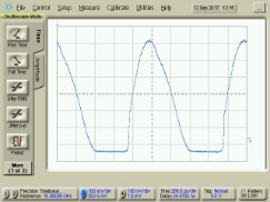
1 Ghz +22 dBm Sine Wave Input graph for NLTL-6273SM
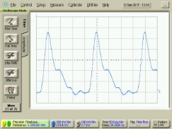
NLTL Output for 1GHz +22 dBm Sine Wave Input graph for NLTL-6273SM
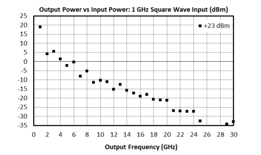
Output Power vs Input Power: 1 GHz Square Wave Input (dBm) graph for NLTL-6273SM
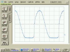
1 GHz +25 dBm Square Wave Input graph for NLTL-6273SM
NLTL Output for 1Ghz +25 dBm Square Wave Input graph for NLTL-6273SM
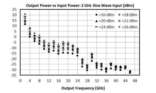
Output Power vs Input Power: 2 GHz Sine Wave Input (dBm) graph for NLTL-6273SM
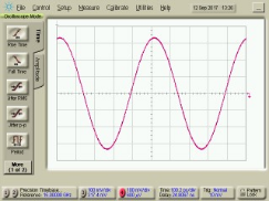
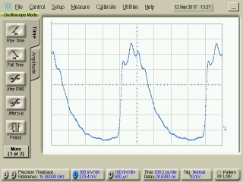
2 GHz +24 dBm Sine Wave Input graph for NLTL-6273SM
NLTL Output for 2GHz +25 dBm Sine Wave Input graph for NLTL-6273SM
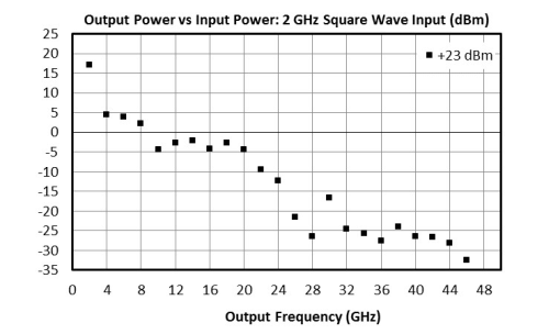
Output Power vs Input Power: 2 GHz Square Wave Input (dBm) graph for NLTL-6273SM
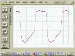
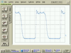
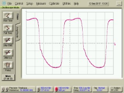
2 GHz +25 dBm Square Wave Input graph for NLTL-6273SM
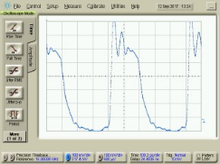
NLTL Output for 2GHz +25 dBm Square Wave Input graph for NLTL-6273SM
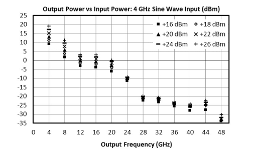
Output Power vs Input Power: 4 GHz Sine Wave Input (dBm) graph for NLTL-6273SM
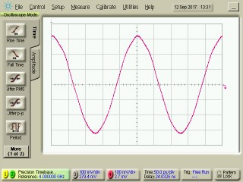
4 GHz +24 dBm Sine Wave Input graph for NLTL-6273SM
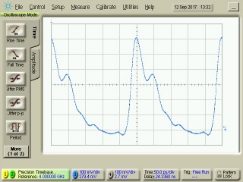
NLTL Output for GHz +24 dBm Sine Wave Input graph for NLTL-6273SM
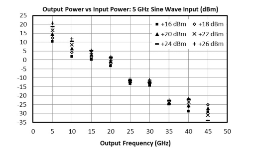
Output Power vs Input Power: 5 GHz Sine Wave Input (dBm) graph for NLTL-6273SM
5 GHz +24 dBm Sine Wave Input graph for NLTL-6273SM
NLTL Output for 5GHz +24 dBm Sine Wave Input graph for NLTL-6273SM
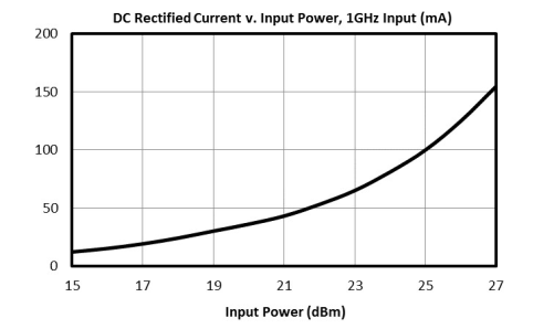
DC Rectified Current v. Input Power, 1 GHz Input (mA) graph for NLTL-6273SM

Typical Performance Plots: Residual Phase Noise

Nltl 6273 Sm Typical Performance Plot Residual

Typical Performance Plots

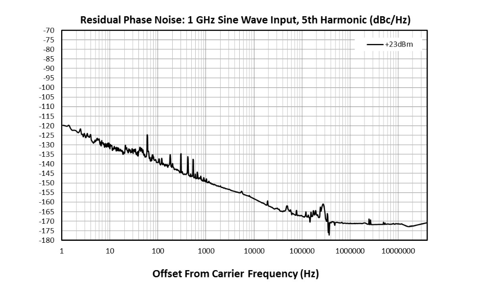
Residual Phase Noise: 1 GHz Sine Wave Input, 5th Harmonic (dBc/Hz) graph for NLTL-6273SM

Specifications

Electrical Specifications

The electrical specifications apply at TA=+25°C in a 50Ω system. Typical data shown is for the NLTL used in the forward direction with a +20 dBm sine wave input. Min and Max limits apply only to our connectorized units and are guaranteed at TA=+25°C. All bare die are 100% DC tested and visually inspected.

ParameterTest ConditionsMinimum
Frequency
(GHz)
Maximum
Frequency
(GHz)
MinTypMaxUnit
Input Frequency Range -- -0.7-5GHz
Input Power -- -16-26dBm
Maximum Output Harmonic for given Input 2 GHz Input
- ---12-
Maximum Output Harmonic for given Input 4 GHz Input
- ---8-
Maximum Output Harmonic for given Input 5 GHz Input
- ---6-
Maximum Output Harmonic for given Input 700 MHz Input
- ---8-
Output Frequency Range -- -0.7-24GHz
Maximum Output Harmonic for given Input 1 GHz Input
- ---24-

The Recommended Operating Conditions indicate the limits, inside which the device should be operated, to guarantee the performance given in Electrical Specifications Operating outside these limits may not necessarily cause damage to the device, but the performance may degrade outside the limits of the electrical specifications. For limits, above which damage may occur, see Absolute Maximum Ratings.

ParameterMinNominalMaxUnit
Ambient Temperature -5525100°C
Input Power 16-26dBm

Absolute Maximum Ratings

The Absolute Maximum Ratings indicate limits beyond which damage may occur to the device. If these limits are exceeded, the device may be inoperable or have a reduced lifetime.

ParameterMaximum RatingUnit
Maximum Operating Temperature 100°C
Maximum Storage Temperature 125°C
Minimum Operating Temperature -55°C
Minimum Storage Temperature -65°C

Package Information

ParameterDetailsRating
Dimensions-5 x 5 mm
Moisture Sensitivity Level-MSL 1

Sequencing Requirements

This is a passive NLTL that requires no external DC bias. Self-bias of the diodes is sufficient for operation. It is not required, but is recommended to provide a 50Ω termination to each port before applying RF power.

Port Configuration and Functions

Port Diagram

A bottom-up view of the NLTL-6273’s SM package outline drawing is shown below. The NLTL should only be used in the forward direction, with the input and output ports given in Port Functions.

Diagram of the port configuration for NLTL-6273SM

Port Functions

PortFunctionDescriptionDC Equivalent
Circuit
GNDGround SM package ground path is provided through the ground paddle.Equivalent circuit for the Ground
Pin 18Output Pin 18 is diode connected for the SM package.Equivalent circuit for the Output
Pin 2Input Pin 2 is diode connected for the SM package.Equivalent circuit for the Input

Operation

Application Information

Nltl 6273 Sm Typical App Info

Detailed Description

NLTL-6273SM belongs to Marki Microwave’s NLTL family of multipliers and non-linear transmission lines. The NLTL product line consists of passive GaAs MMIC non-linear transmission lines designed and fabricated with GaAs Schottky diode based varactors. NLTLs take an input signal and create an impulse train of harmonics. Harmonic outputs up to and beyond 24 GHz are generated by the NLTL. The NLTL-6273SM is the packaged 5 mm QFN version of the NLTL-6273CH.

Port 1 supports L and S band input signals. Port 2 will output integer multiples of the input signal (i.e., x2, x3, x4, …, x24) up to the 24th output harmonic or a maximum of 24 GHz. Higher harmonics can be generated but will be at a lower efficiency.

The operating conditions of the NLTL are extremely important to optimize performance. High power inputs will increase the output power observed; however, the conversion efficiency will decrease. This is increasingly true for higher input frequencies and at input powers above the recommended limit. Optimal conversion efficiency of the NLTL is achieved using a square wave input with a fast rise time. Doing so causes a degradation in the 2nd output harmonic but otherwise improves the conversion efficiency at all other harmonics.

NLTL-6273SM requires no external DC bias. The self-bias of the diodes caused by the rectified RF input signal is sufficient for operation. For the best performance, optimization of the DC return path is recommended for each specific application to optimize the harmonic output power distribution.

The phase noise of a non-linear transmission line is outstanding. If verification of performance is necessary, the application circuit used and input conditions are extremely important. NLTLs are AM sensitive. If there is excessive AM noise on the input of the NLTL, observing the output of the NLTL will show excessive PM/phase noise because of the high AM to PM conversion property of NLTLs.

Application Circuit

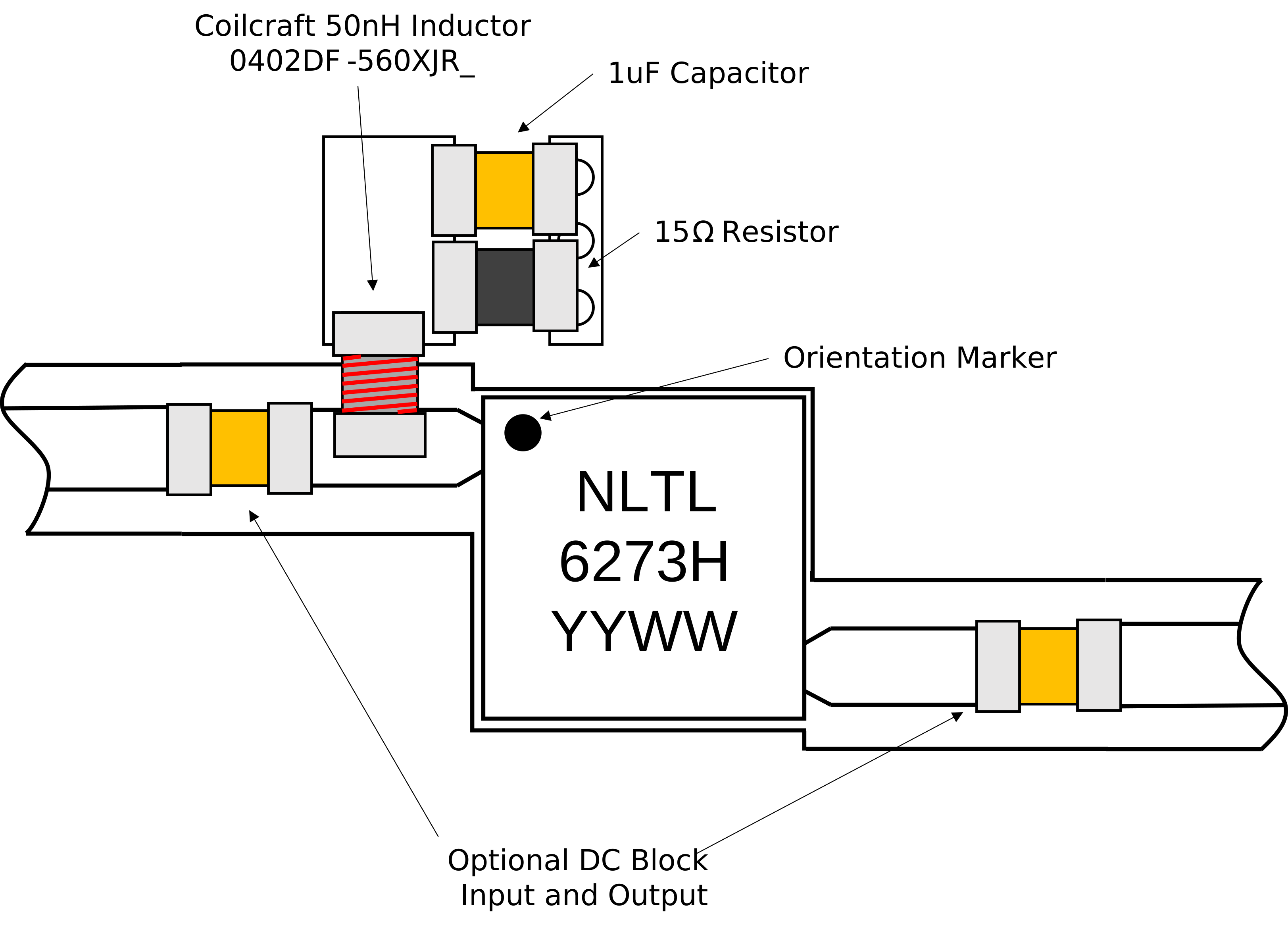
Application Circuit for NLTL-6273SM

Application Circuit Description

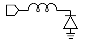
DC Path to Ground — An RF choke followed by a 15 Ω resistor should be used to provide a DC path to ground on the input port of the NLTL. A shunt 1 μF capacitor is used to filter noise generated by the resistor. This forms the circuit which self-biases the NLTL. The DC return to ground removes DC rectified current created by high power RF signal injection. The DC path to ground is provided within the S package. A conical coil inductor is recommended to push the self-resonance frequency of the inductor past the operating bandwidth of the NLTL. The recommended inductance value of the conical coil inductor is 50nH or higher.

Blocking Capacitor — A DC blocking capacitor on the output of the NLTL-6273SM’s integrated circuit is necessary to prevent unwanted DC current flow from or to the output. If there is a DC signal on the input, place a DC block on the input to avoid disrupting the self-biasing of the diodes.

Mechanical Data

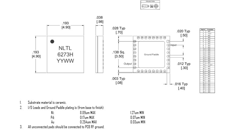
Outline Drawing

Download : Outline 2D Drawing Outline 3D Drawing Outline 3D STP

Outline Drawing

Evaluation Board

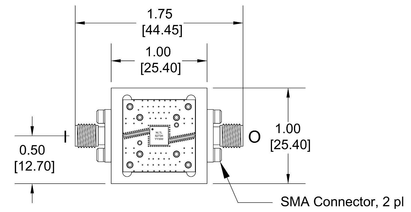
Evaluation Board - Outline Drawing

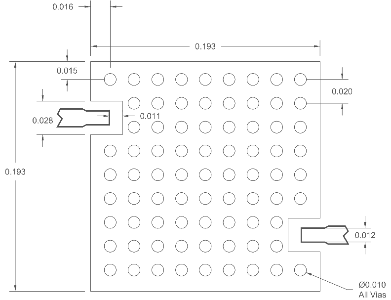
Outline Drawing

Revision History

Revision CodeRevision DateComment
-2017-10-01Datasheet Initial Release
A2017-10-01Corrected typos
B2019-08-01Added DC Current Plot

DISCLAIMER

MARKI MICROWAVE, LLC., (“MARKI”) PROVIDES TECHNICAL SPECIFICATIONS AND DATA (INCLUDING DATASHEETS), APPLICATION OR OTHER DESIGN ADVICE, WEB TOOLS, AND OTHER INFORMATION AND RESOURCES “AS IS” AND WITH ALL FAULTS. MARKI DISCLAIMS ALL WARRANTIES, EXPRESS OR IMPLIED, INCLUDING, WITHOUT LIMITATION, ANY IMPLIED WARRANTIES OF MERCHANTABILITY, FITNESS FOR A PARTICULAR PURPOSE, OR NON-INFRINGEMENT.

These resources are intended for developers skilled in the art designing with Marki products. You are solely responsible for (1) selecting the appropriate products for your application, (2) designing, validating, and testing your application, and (3) ensuring your application meets applicable standards and other requirements. Marki makes no guarantee regarding the suitability of its products for any particular purpose, nor does Marki assume any liability whatsoever arising out of your use or application of any Marki product.

Marki grants you permission to use these resources only for development of an application that uses Marki products. Other reproduction or use of these resources is strictly prohibited. No license is granted to any other Marki intellectual property or to any third-party intellectual property. Marki reserves the right to make changes to the product(s) or information contained herein without notice.

MARKI MICROWAVE, M wave logo, FastSwitch, and T3 MIXER are trademarks or registered trademarks of Marki Microwave, LLC. All other trademarks used are the property of their respective owners.

© 2017, 2019, Marki Microwave, LLC