Rev: - | Copyright © 2024 Marki Microwave LLC.

General Description

The MMPX-00001PSM is a MMIC surface mount quadplexer capable of multiplexing DC-4 GHz / 6-8 GHz / 10-12 GHz / 14-16 GHz signals. Passive GaAs MMIC technology allows production of smaller filter constructions that replace larger form factor circuit board constructions. Tight fabrication tolerances allow for less unit-to-unit variation than traditional filter technologies. The MMPX-00001PSM is available as a 6x6mm QFN. Low unit to unit variation allows for accurate simulations using the provided SnP files taken from measured production units.

Features

  • Excellent Return Loss
  • 9 GHz crossover frequency
  • High Band-Band Isolation

Functional Block Diagram

Block Diagram
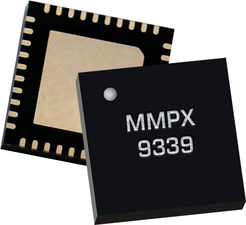
Photo of MMPX-00001PSM

Electrical Performance Summary

ParameterTypUnit
Frequency Range0 to 16GHz
Band 3 10 to 12GHz
Band 1 0 to 4GHz
Band 2 6 to 8GHz
Band 4 14 to 16GHz

Summary only – refer to the Electrical Specifications, Absolute Maximum Ratings, and Recommended Operating Range tables for complete details.

Part Ordering Options

Part NumberDescriptionPackageGreen StatusProduct LifecycleExport Classification
MMPX-00001PSMPassive MMIC DC-16 GHz QuadplexerQFN

RoHS

REACH

ReleasedEAR99
EVB-MMPX-00001PEvaluation Board, Passive MMIC 2-16 GHz QuadplexerEVB

RoHS

REACH

ReleasedEAR99

Table Of Contents

Typical Performance Plots

Typical performance plots are evaluation board measurements with fixturing to the device pads de-embedded.

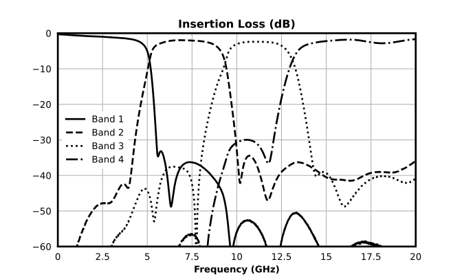
Insertion Loss (dB) graph for MMPX-00001PSM
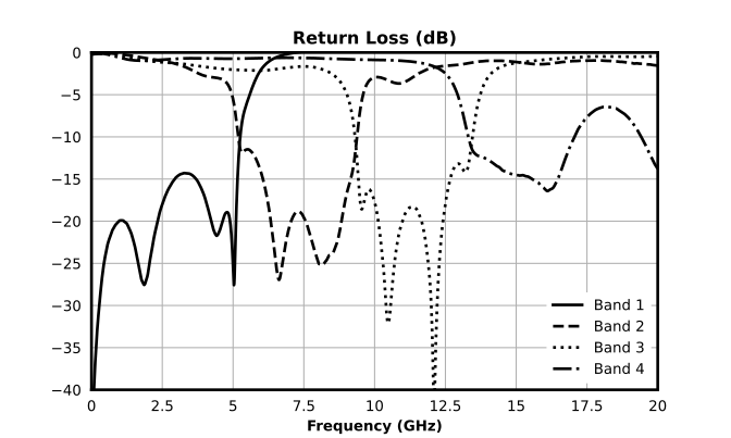
Return Loss (dB) graph for MMPX-00001PSM
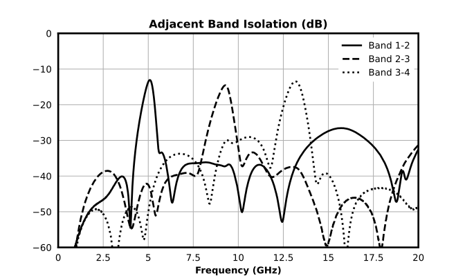
Adjacent Isolation (dB) graph for MMPX-00001PSM
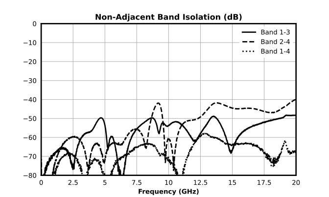
Non-Adjacent Isolation (dB) graph for MMPX-00001PSM
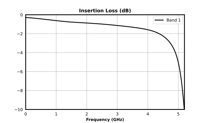
Band 1 Insertion Loss (dB) graph for MMPX-00001PSM
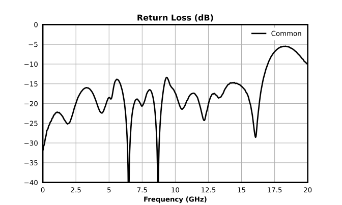
Common Port Return Loss (dB) graph for MMPX-00001PSM
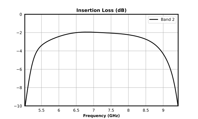
Band 2 Insertion Loss (dB) graph for MMPX-00001PSM
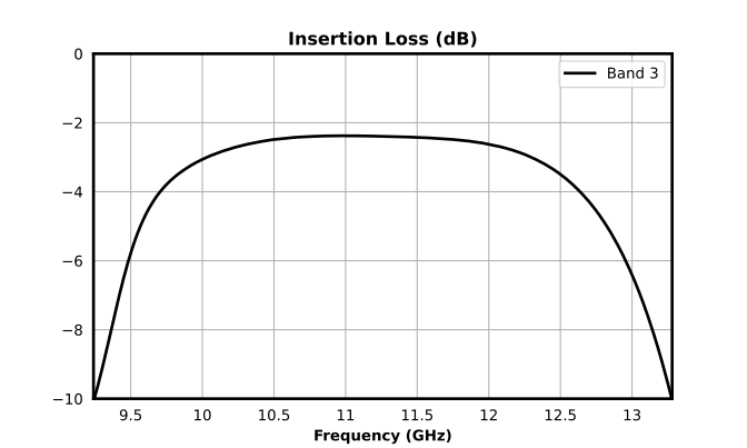
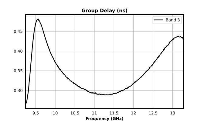
Band 3 Insertion Loss (dB) graph for MMPX-00001PSM
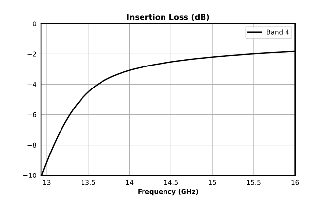
Insertion Loss (dB) graph for MMPX-00001PSM
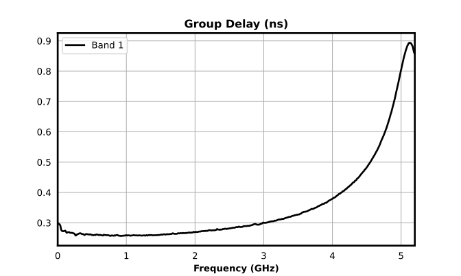
Band 1 Group Delay (ps) graph for MMPX-00001PSM

Specifications

Electrical Specifications

The electrical specifications apply at TA=+25°C in a 50Ω system. Typical data shown is for the filter in a PSM package with a sine wave input applied to Pin 15. Min and Max limits are guaranteed at TA=+25°C.

ParameterTest ConditionsMinimum
Frequency
(GHz)
Maximum
Frequency
(GHz)
MinTypMaxUnit
Frequency Range-0 16---GHz
1 dBc High Passband Temp = 25°C
- -0.01--GHz
3 dBc High Passband Temp = 25°C
- -1.72--GHz
30 dBc High Pass Rejection Point Temp = 25°C
- -1.72--GHz
High Passband Return Loss Temp = 25°C
- --21-dB
High Pass Isolation Temp = 25°C
- --59-dB
High Pass Group Delay Temp = 25°C
- --267-ps
1 dBc Low Passband Temp = 25°C
- ---12.46GHz
3 dBc Low Passband Temp = 25°C
- ---12.87GHz
30 dBc Low Pass Rejection Point Temp = 25°C
- ---14.11GHz
Low Passband Return Loss Temp = 25°C
- --21-dB
Low Pass Isolation Temp = 25°C
- --54-dB
Low Pass Group Delay Temp = 25°C
- --310-ps
Crossover Frequency Temp = 25°C
- --6.85-GHz
Common Port Return Loss Temp = 25°C
- --20-dB
Impedance Temp = 25°C
- --50-Ω
Band 1 -- -0-4GHz
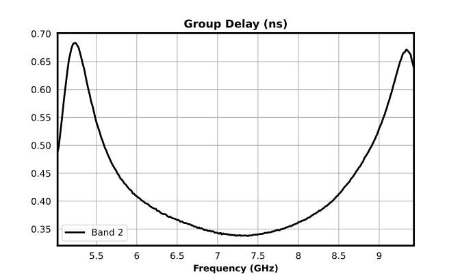
Band 2 -- -6-8GHz
Band 3 -- -10-12GHz
Band 4 -- -14-16GHz
Center Frequency Band 1
0 4-2-GHz
Center Frequency Band 2
6 8-7-GHz
Center Frequency Band 3
10 12-11.1-GHz
Center Frequency Band 4
14 16-15-GHz
Cross Over Frequency Band 1 to Band 2
- --5.1-GHz
Cross Over Frequency Band 2 to Band 3
- --9.3-GHz
Cross Over Frequency Band 3 to Band 4
- --13.1-GHz
Group Delay Band 1
0 4-267-ps
Group Delay Band 2
6 8-363-ps
Group Delay Band 3
10 12-311-ps
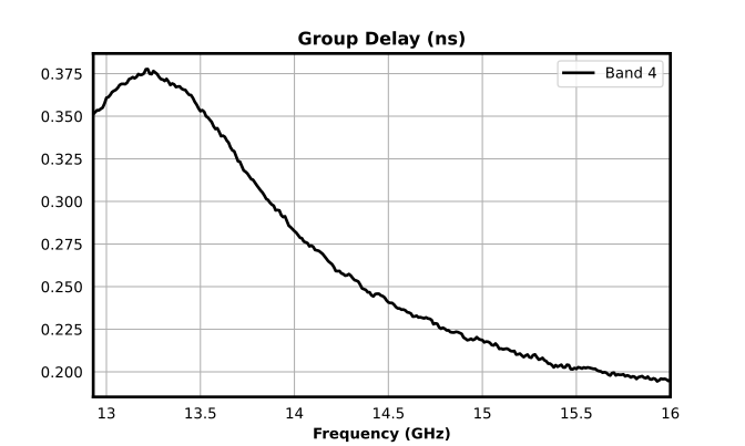
Group Delay Band 4
14 16-149-ps
Insertion Loss @ fc Band 1
0 4-0.8-dB
Insertion Loss @ fc Band 2
6 8-2-dB
Insertion Loss @ fc Band 3
10 12-2.4-dB
Insertion Loss @ fc Band 4
14 16-2.1-dB
Return Loss Band 1
0 4-21-dB
Return Loss Band 2
6 8-19-dB
Return Loss Band 3
10 12-19-dB
Return Loss Band 4
14 16-8-dB

Absolute Maximum Ratings

The Absolute Maximum Ratings indicate limits beyond which damage may occur to the device. All Absolute Maximum Ratings are individual and should not be met in parallel. If these limits are exceeded, the device may be inoperable or have a reduced lifetime.

ParameterMaximum RatingUnit
Maximum Operating Temperature 100°C
Maximum Storage Temperature 125°C
Minimum Operating Temperature -55°C
Minimum Storage Temperature -65°C
RF Power Handling 30dBm

Package Information

ParameterDetailsRating
ESD< 50 VoltsHBM 0Z
Dimensions-6 x 6 mm
Moisture Sensitivity Level-MSL 1

Port Configuration and Functions

Port Functions

PortFunctionDescriptionDC Equivalent
Circuit
Ground PaddleGround PSM package ground path is provided through the substrate and ground bond pads.Equivalent circuit for the Ground
Pin 15Input/Common Pin 15 is DC short to Pin 29 and open to all other ports and ground.Equivalent circuit for the Input/Common
Pin 2Band 4 Input/Output Pin 2 is DC open to all other ports and ground.Equivalent circuit for the Band 4 Input/Output
Pin 29Band 1 Input/Output Pin 29 is DC short to Pin 15 and open to all other ports and ground.Equivalent circuit for the Band 1 Input/Output
Pin 33Band 2 Input/Output Pin 33 is DC open to all other ports and ground.Equivalent circuit for the Band 2 Input/Output
Pin 37Band 3 Input/Output Pin 37 is DC open to all other ports and ground.Equivalent circuit for the Band 3 Input/Output

Mechanical Data

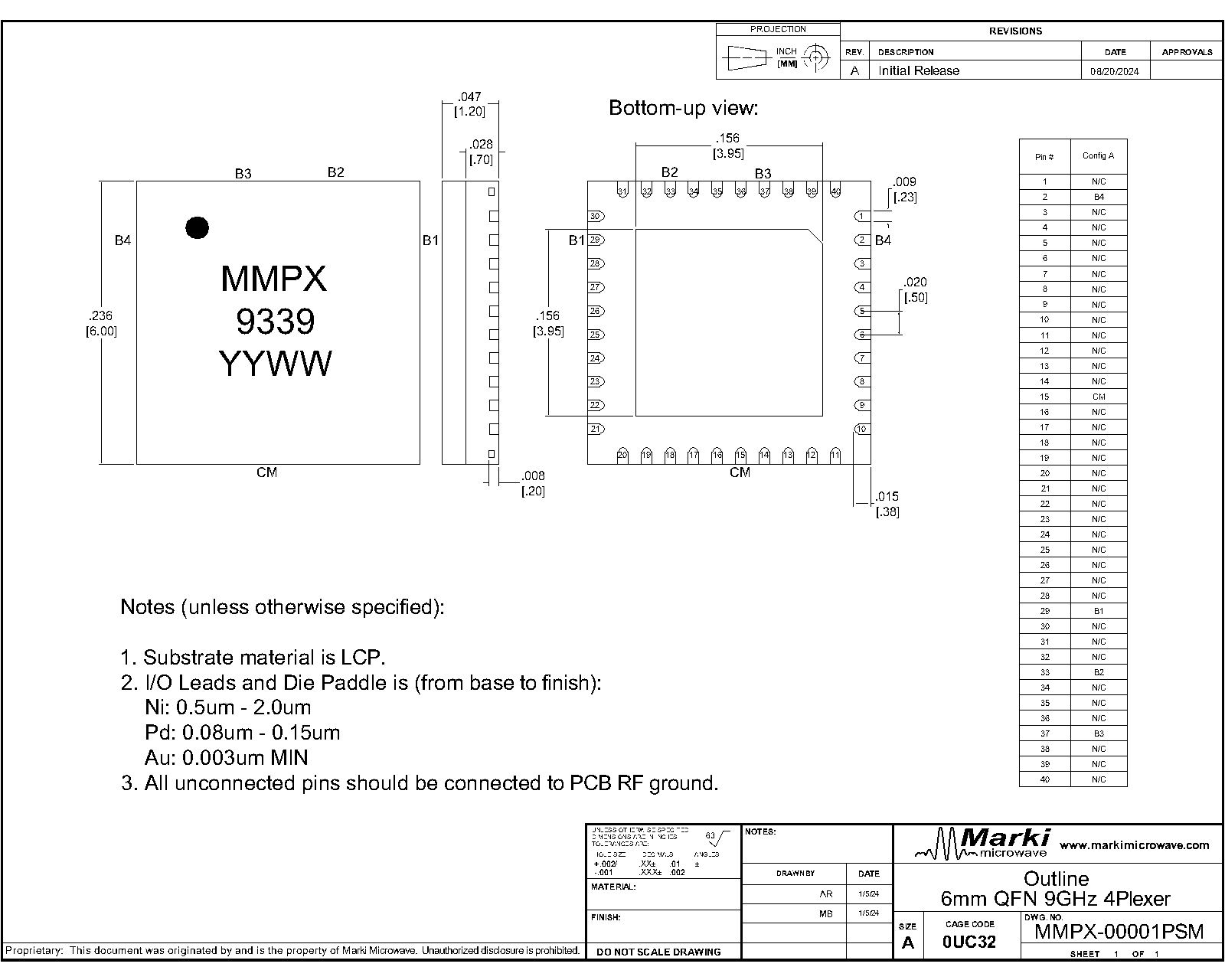
Outline Drawing

Download : Outline 2D Drawing Outline 3D STP

Outline Drawing

Evaluation Board

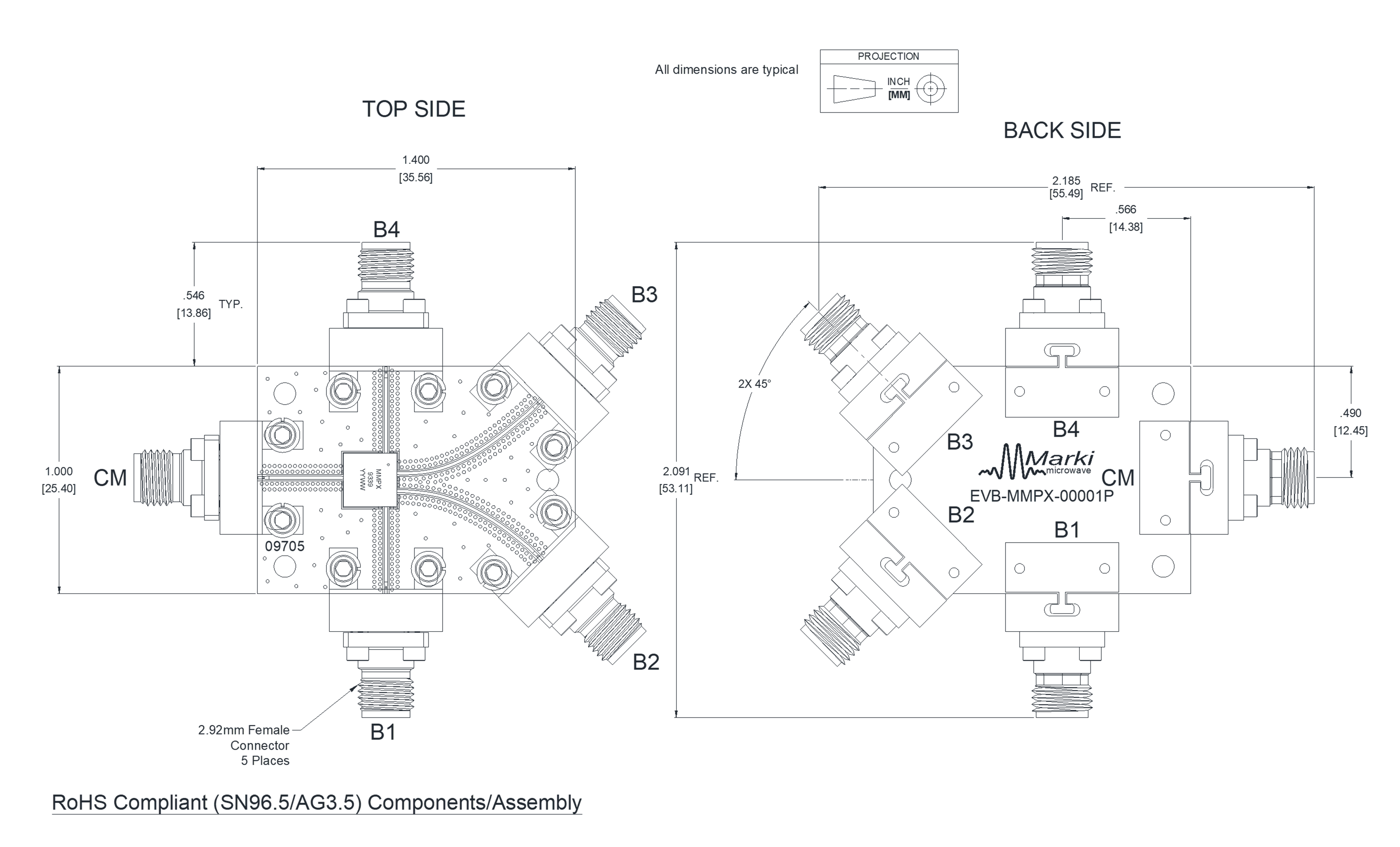
Evaluation Board - Outline Drawing

Outline Drawing

Revision History

Revision CodeRevision DateComment
-2024-07-09Datasheet Initial Release

DISCLAIMER

MARKI MICROWAVE, LLC., (“MARKI”) PROVIDES TECHNICAL SPECIFICATIONS AND DATA (INCLUDING DATASHEETS), APPLICATION OR OTHER DESIGN ADVICE, WEB TOOLS, AND OTHER INFORMATION AND RESOURCES “AS IS” AND WITH ALL FAULTS. MARKI DISCLAIMS ALL WARRANTIES, EXPRESS OR IMPLIED, INCLUDING, WITHOUT LIMITATION, ANY IMPLIED WARRANTIES OF MERCHANTABILITY, FITNESS FOR A PARTICULAR PURPOSE, OR NON-INFRINGEMENT.

These resources are intended for developers skilled in the art designing with Marki products. You are solely responsible for (1) selecting the appropriate products for your application, (2) designing, validating, and testing your application, and (3) ensuring your application meets applicable standards and other requirements. Marki makes no guarantee regarding the suitability of its products for any particular purpose, nor does Marki assume any liability whatsoever arising out of your use or application of any Marki product.

Marki grants you permission to use these resources only for development of an application that uses Marki products. Other reproduction or use of these resources is strictly prohibited. No license is granted to any other Marki intellectual property or to any third-party intellectual property. Marki reserves the right to make changes to the product(s) or information contained herein without notice.

MARKI MICROWAVE, M wave logo, FastSwitch, and T3 MIXER are trademarks or registered trademarks of Marki Microwave, LLC. All other trademarks used are the property of their respective owners.

© 2024, Marki Microwave, LLC