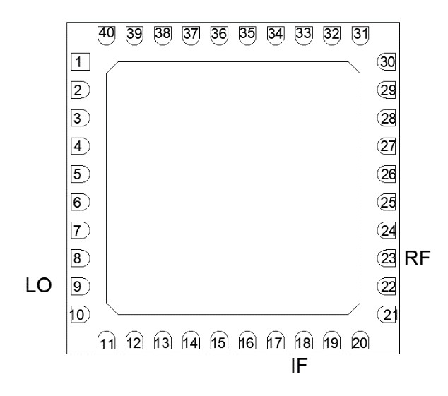
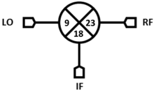
Port Diagram
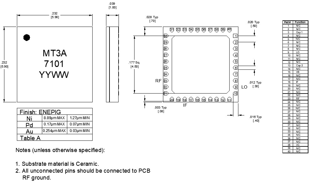
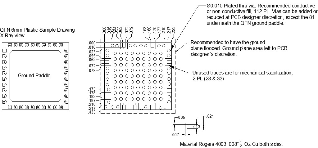
A top-down x-ray view of the MT3A-0113HCSM’s CSM Package outline drawing is shown below. The MT3A-0113HCSM has the input and output ports given in Port Functions.
Sales: 408-778-9952 | General: 408-778-4200 | Fax: 408-778-4300
Sales & Customer Support: [email protected]
Tech Support: [email protected]
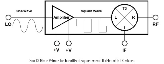
The MT3A-0113HCSM is a versatile, robust, and broadband Two-Tone-Terminator mixer integrated with a low phase noise LO driver amplifier. The MT3A-0113HCSM employs the most sophisticated mixer on the market today and offers unparalleled performance when compared to all other mixer technologies. The MT3A-0113HCSM delivers exceptional IMD suppression with low conversion loss and high IP3. The integrated positive bias only LO amplifier allows for high linearity with LO drive levels down to just +5dBm.
| Part Number | Description | Package | Green Status | Product Lifecycle | Export Classification |
|---|---|---|---|---|---|
| MT3A-0113HCSM | Two-Tone-Terminator Mixer/LO Amplifier | QFN | REACH RoHS | Released | EAR99 |
| EVB-MT3A-0113HC | Evaluation Board, Two-Tone-Terminator 1.5 - 13 GHz Mixer. | EVB | Non-RoHS | Released | EAR99 |
MT3A-0113HCSM
Two-Tone-Terminator Mixer/LO Amplifier
| Revision Code | Revision Date | Comment |
|---|---|---|
| - | 2021-10-01 | Datasheet Initial Release |
MT3A-0113HCSM
Two-Tone-Terminator Mixer/LO Amplifier
A top-down x-ray view of the MT3A-0113HCSM’s CSM Package outline drawing is shown below. The MT3A-0113HCSM has the input and output ports given in Port Functions.
MT3A-0113HCSM
Two-Tone-Terminator Mixer/LO Amplifier
| Port | Function | Description | DC Equivalent Circuit |
|---|---|---|---|
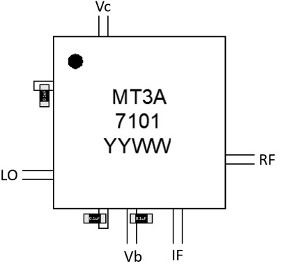
| GND | Ground | IC backside must be connected to a DC/RF ground with high thermal and electrical conductivity. |  |
| Pin 13 | Cap 2 | Pin 13 allows the user to attach additional off chip bypass capacitance to provide adequate low frequency AC grounding termination to the input matching network. The value should be at least 100nF. |  |
| Pin 15 | VB | Pin 15 is the DC voltage bias for the current mirror that controls collector current supplied to the amplifier. Larger voltages result in a higher current draw through port VC, effectively functioning as a gain control pin of the amplifier. |  |
| Pin 18 | IF | Pin 18 is DC blocked and AC matched to 50 Ohms from 500 MHz to 8.5 GHz. |  |
| Pin 23 | RF | Pin 23 is DC short to ground and AC matched to 50 Ohms from 1.5 GHz to 13 GHz. Blocking capacitor is optional. |  |
| Pin 3 | Cap 1 | Pin 3 allows the user to attach additional off chip bypass capacitance to provide adequate low frequency AC grounding termination to the input matching network. The value should be at least 100nF. |  |
| Pin 38 | VC | Pin 38 is the DC voltage supply that supplies the amplifier’s collector current. |  |
| Pin 9 | LO | The LO port is DC blocked and AC matched to 50 Ohms from 1.5 GHz to 13 GHz. |  |
MT3A-0113HCSM
Two-Tone-Terminator Mixer/LO Amplifier
The Absolute Maximum Ratings indicate limits beyond which damage may occur to the device. If these limits are exceeded, the device may be inoperable or have a reduced lifetime.
| Parameter | Maximum Rating | Unit |
|---|---|---|
| DC Bias Current | 150 | mA |
| DC Voltage on VB or VC | 8 | V |
| LO Power Handling | 15 | dBm |
| Maximum Operating Temperature | 85 | °C |
| Maximum Storage Temperature | 125 | °C |
| Max Junction Temperature for MTTF> 1E6 hours | 125 | °C |
| Max Power Dissipation for MTTF of 1E6 hours at 85˚C Baseplate Temperature | 650 | mW |
| Minimum Operating Temperature | -55 | °C |
| Minimum Storage Temperature | -65 | °C |
| RF Power Handling | 25 | dBm |
| θJC, Junction to Case Thermal Resistance | 61 | ºC/W |
| Parameter | Details | Rating |
|---|---|---|
| ESD | 250 to < 500 Volts | HBM Class 1A |
| Dimensions | - | 6 x 6 mm |
| Moisture Sensitivity Level | - | MSL 1 |
| Parameter | Min | Nominal | Max | Unit |
|---|---|---|---|---|
| Ambient Temperature | 55 | 25 | 85 | °C |
| LO Input Power | 5 | 12 | 15 | dBm |
| Positive DC Voltage (VC) 1 | 5 | 7 | 8 | V |
| Positive DC Current Mirror Voltage (VB) | 5 | 6 | 8 | V |
| Current Draw | 80 | 120 | 150 | mA |
[1] There is no sequencing required to apply DC or RF power to the mixer.
MT3A-0113HCSM
Two-Tone-Terminator Mixer/LO Amplifier
The electrical specifications apply at TA=+25°C in a 50Ω system. Typical data shown is for a down conversion application with a +12dBm sine wave LO input to the integrated LO driver amp biased at +6VB/+7VC.
| Parameter | Test Conditions | Min | Typ | Max | Unit |
|---|---|---|---|---|---|
| IF Frequency Range | - | 0.5 | - | 8.5 | GHz |
| LO Frequency Range | - | 1.5 | - | 13 | GHz |
| RF Frequency Range | - | 1.5 | - | 13 | GHz |
| Conversion Loss 1 | RF/LO = 1.5 - 13 GHz I = 0.5 - 2 GHz | - | 9.5 | 14 | dB |
| Conversion Loss | RF/LO = 1.5 - 13 GHz I = 2 – 8.5 GHz | - | 11.5 | - | dB |
| Current Consumption | +6.0VB/+7.0VC | 80 | 120 | 150 | mA |
| Input IP3 | RF/LO = 1.5 - 13 GHz I = 0.5 - 2 GHz | - | 28 | - | dBm |
| Input P0.1 dB | - | - | 13 | - | dBm |
| Noise Figure 2 | RF/LO = 1.5 - 13 GHz I = 0.5 - 2 GHz | - | 10 | - | dB |
[1] Measured as a down converter to a fixed 1 GHz IF.
[2] Mixer Noise Figure typically measures within 0.5 dB of conversion loss for IF frequencies greater than 5 MHz.
MT3A-0113HCSM
Two-Tone-Terminator Mixer/LO Amplifier


MT3A-0113HCSM
Two-Tone-Terminator Mixer/LO Amplifier


MT3A-0113HCSM
Two-Tone-Terminator Mixer/LO Amplifier
MT3A-0113HCSM
Two-Tone-Terminator Mixer/LO Amplifier
MT3A-0113HCSM
Two-Tone-Terminator Mixer/LO Amplifier
MT3A-0113HCSM
Two-Tone-Terminator Mixer/LO Amplifier
MT3A-0113HCSM
Two-Tone-Terminator Mixer/LO Amplifier