Port Diagram
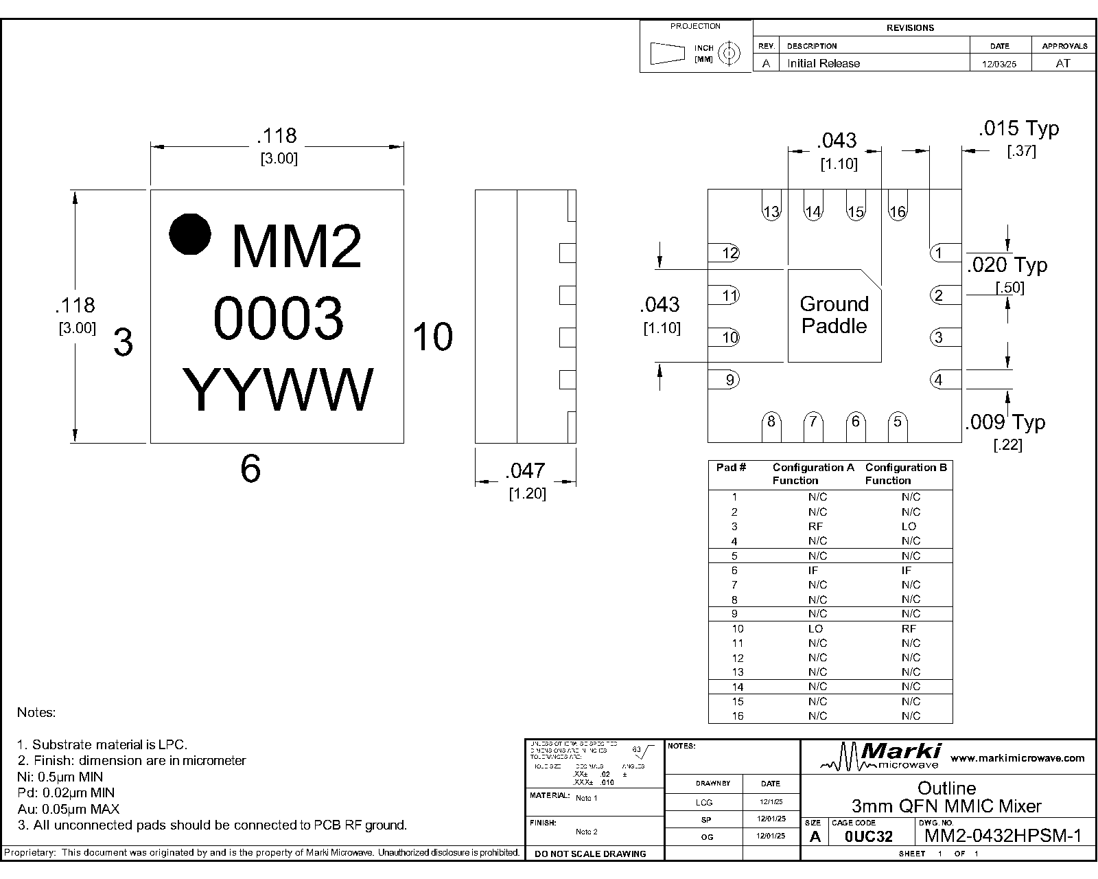
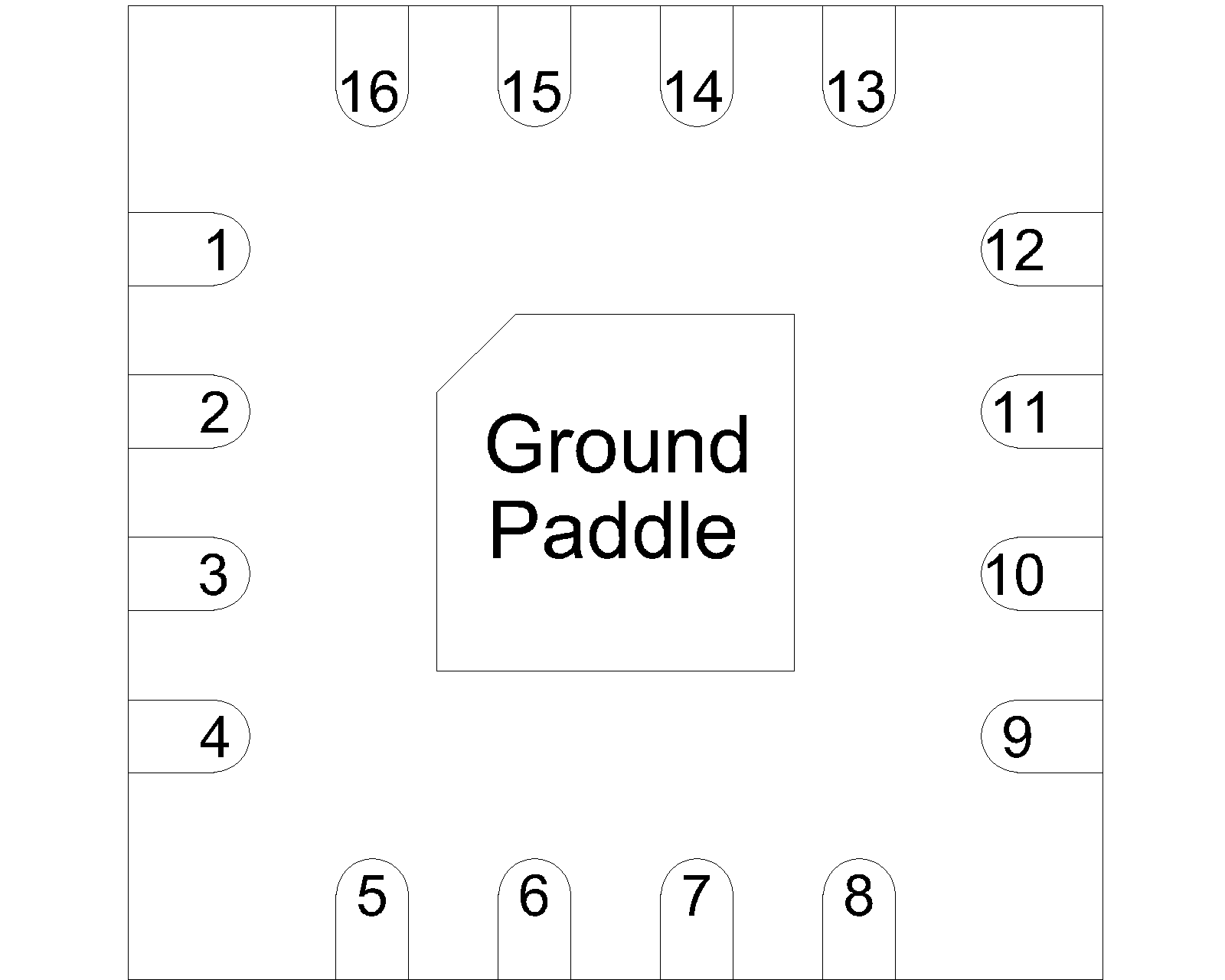
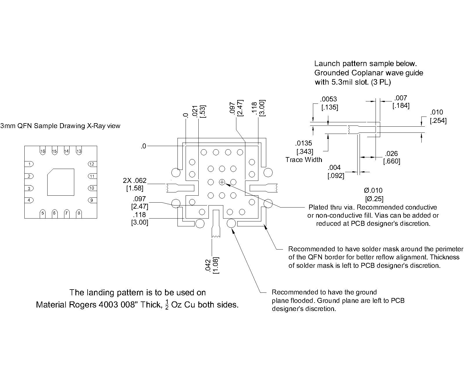
A top-down x-ray view of the package is shown below.
Sales: 408-778-9952 | General: 408-778-4200 | Fax: 408-778-4300
Sales & Customer Support: [email protected]
Tech Support: [email protected]
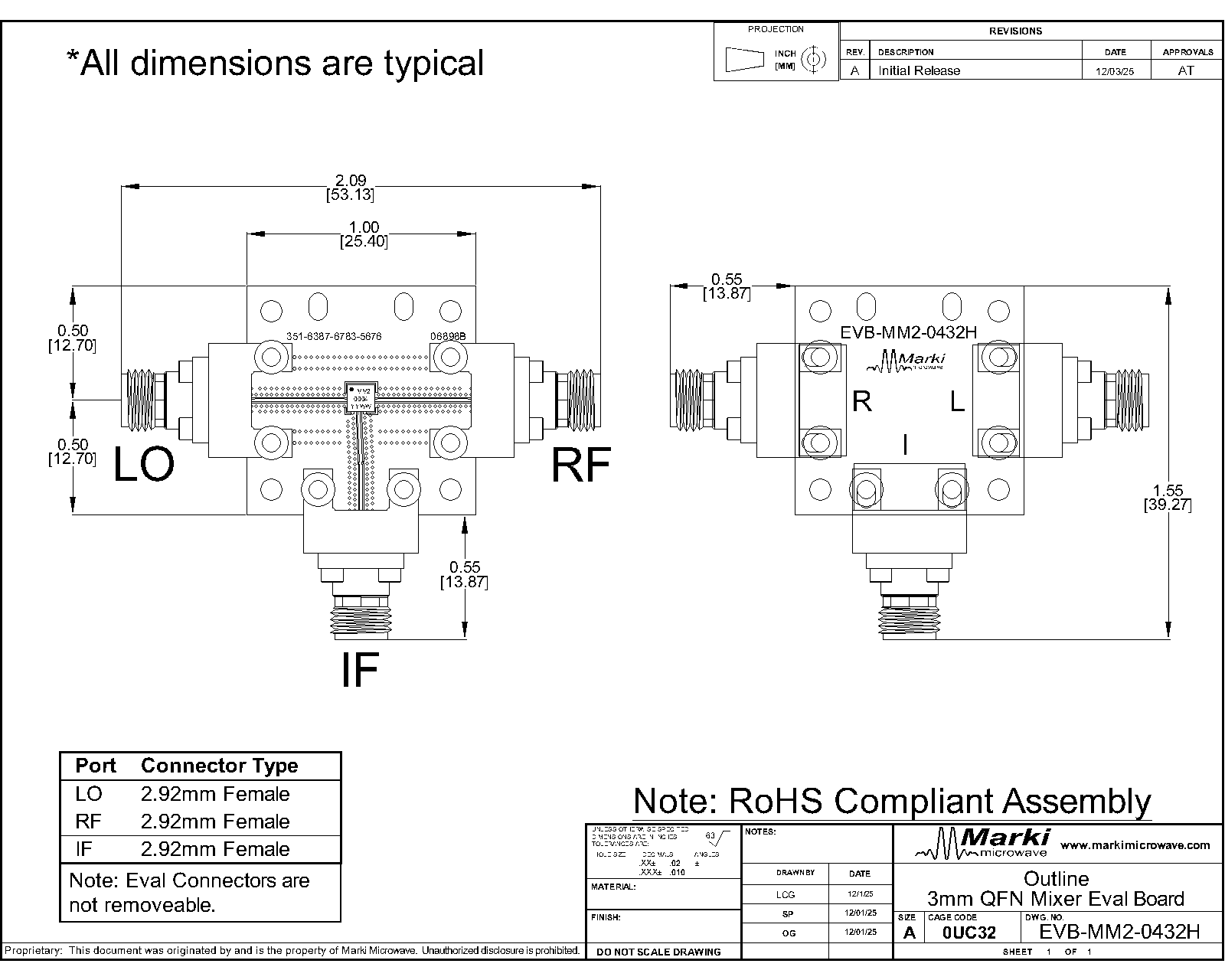
The MM2-0432HPSM-1 is a passive GaAs MMIC triple-balanced mixer designed with broadband operation from 4 to 32 GHz. It delivers low conversion loss, high linearity, and excellent port-to-port isolation. The device supports a wide LO input power range of +15 to +21 dBm (nominal +18 dBm), providing flexibility across system implementations. Packaged in a 3 × 3 mm QFN, the MM2-0432HPSM-1 enables compact, repeatable implementations in space-constrained RF assemblies. Evaluation boards are available.

| Part Number | Description | Package | Green Status | Product Lifecycle | Export Classification |
|---|---|---|---|---|---|
| MM2-0432HPSM-1 | GaAs MMIC Triple Balanced Mixer | PSM | REACH RoHS | Released | EAR99 |
| MM2-0432HPSM-2 | GaAs MMIC Triple Balanced Mixer | PSM | REACH RoHS | Released | EAR99 |
| EVB-MM2-0432HP | Evaluation Board, GaAs MMIC Mixer | EVB | RoHS REACH | Released | EAR99 |
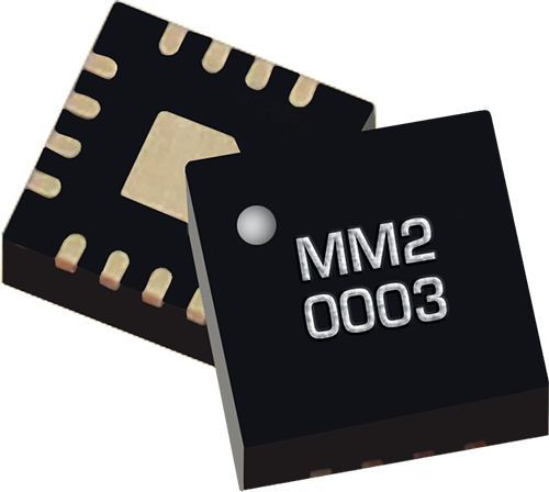
MM2-0432HPSM-1
GaAs MMIC Triple Balanced Mixer
| Revision Code | Revision Date | Comment |
|---|---|---|
| - | 2026-05-04 | Initial Release |
MM2-0432HPSM-1
GaAs MMIC Triple Balanced Mixer
A top-down x-ray view of the package is shown below.
| Port | Function | Description | DC Equivalent Circuit |
|---|---|---|---|
| Pin 10 | LO | Pin 10 is DC short and AC matched to 50 Ω from 2 to 34 GHz. Blocking capacitor is optional. |  |
| Pin 3 | RF | Pin 3 is DC short and AC matched to 50 Ω from 4 to 32 GHz. Blocking capacitor is optional. | |
| Pin 6 | IF | Pin 6 is DC coupled to the diodes. Blocking capacitor is optional. |  |
MM2-0432HPSM-1
GaAs MMIC Triple Balanced Mixer
| Port | Function | Description | DC Equivalent Circuit |
|---|---|---|---|
| Pin 10 | RF | Pin 10 is DC short and AC matched to 50 Ω from 4 to 32 GHz. Blocking capacitor is optional. | |
| Pin 3 | LO | Pin 3 is DC short and AC matched to 50 Ω from 2 to 34 GHz. Blocking capacitor is optional. | |
| Pin 6 | IF | Pin 6 is DC coupled to the diodes. Blocking capacitor is optional. | |
MM2-0432HPSM-1
GaAs MMIC Triple Balanced Mixer
| Parameter | Maximum Rating | Unit |
|---|---|---|
| Maximum Operating Temperature | 100 | °C |
| Maximum Storage Temperature | 125 | °C |
| Minimum Operating Temperature | -55 | °C |
| Minimum Storage Temperature | -65 | °C |
| Pin 10 DC Current | 24 | mA |
| Pin 3 DC Current | 21 | mA |
| Pin 6 DC Current | 15 | mA |
| Parameter | Details | Rating |
|---|---|---|
| ESD | 250 to < 500 Volts | HBM Class 1A |
| Dimensions | - | 3 x 3 mm |
| Moisture Sensitivity Level | - | MSL 1 |
| Parameter | Min | Nominal | Max | Unit |
|---|---|---|---|---|
| LO Input Power | 15 | 18 | 21 | dBm |
MM2-0432HPSM-1
GaAs MMIC Triple Balanced Mixer
Specifications guaranteed from -55 to +100°C, measured in a 50Ω system. Specifications are shown for Configurations A (B). RF testing is performed on a sample basis to verify conformance to datasheet guaranteed specifications. Consult factory for more information.
| Parameter | Port Configuration | Test Conditions | Min | Typ | Max | Unit |
|---|---|---|---|---|---|---|
| Conversion Loss | A | RF=4-32GHz LO=6-34GHz IF=2GHz LO Drive Level=+18dBm | - | 6 | - | dB |
| Input IP3 | A | RF=4-32GHz LO=6-34GHz IF=2GHz LO Drive Level=+18dBm | - | 22 | - | dBm |
| Input P1dB | A | RF=4-32GHz LO=6-34GHz IF=2GHz LO Drive Level=+18dBm | - | 21 | - | dBm |
| Conversion Loss | B | RF=4-32GHz LO=6-34GHz IF=2GHz LO Drive Level=+18dBm | - | 7 | - | dB |
| Input IP3 | B | RF=4-32GHz LO=6-34GHz IF=2GHz LO Drive Level=+18dBm | - | 24 | - | dBm |
| Input P1dB | B | RF=4-32GHz LO=6-34GHz IF=2GHz LO Drive Level=+18dBm | - | 24 | - | dB |
| RF-IF Isolation | - | RF=4-32GHz LO=6-34GHz IF=2GHz LO Drive Level=+18dBm | - | 40 | - | dB |
| LO-RF Isolation | - | RF=4-32GHz LO=6-34GHz IF=2GHz LO Drive Level=+18dBm | - | 45 | - | dB |
| LO-IF Isolation | - | RF=4-32GHz LO=6-34GHz IF=2GHz LO Drive Level=+18dBm | - | 40 | - | dB |
| RF Frequency Range | - | - | 4 | - | 32 | GHz |
| LO Frequency Range | - | - | 2 | - | 34 | GHz |
| IF Frequency Range | - | - | 2 | - | 8 | GHz |
MM2-0432HPSM-1
GaAs MMIC Triple Balanced Mixer


MM2-0432HPSM-1
GaAs MMIC Triple Balanced Mixer


MM2-0432HPSM-1
GaAs MMIC Triple Balanced Mixer


MM2-0432HPSM-1
GaAs MMIC Triple Balanced Mixer
MM2-0432HPSM-1
GaAs MMIC Triple Balanced Mixer
Download : Footprint Drawing
MM2-0432HPSM-1
GaAs MMIC Triple Balanced Mixer