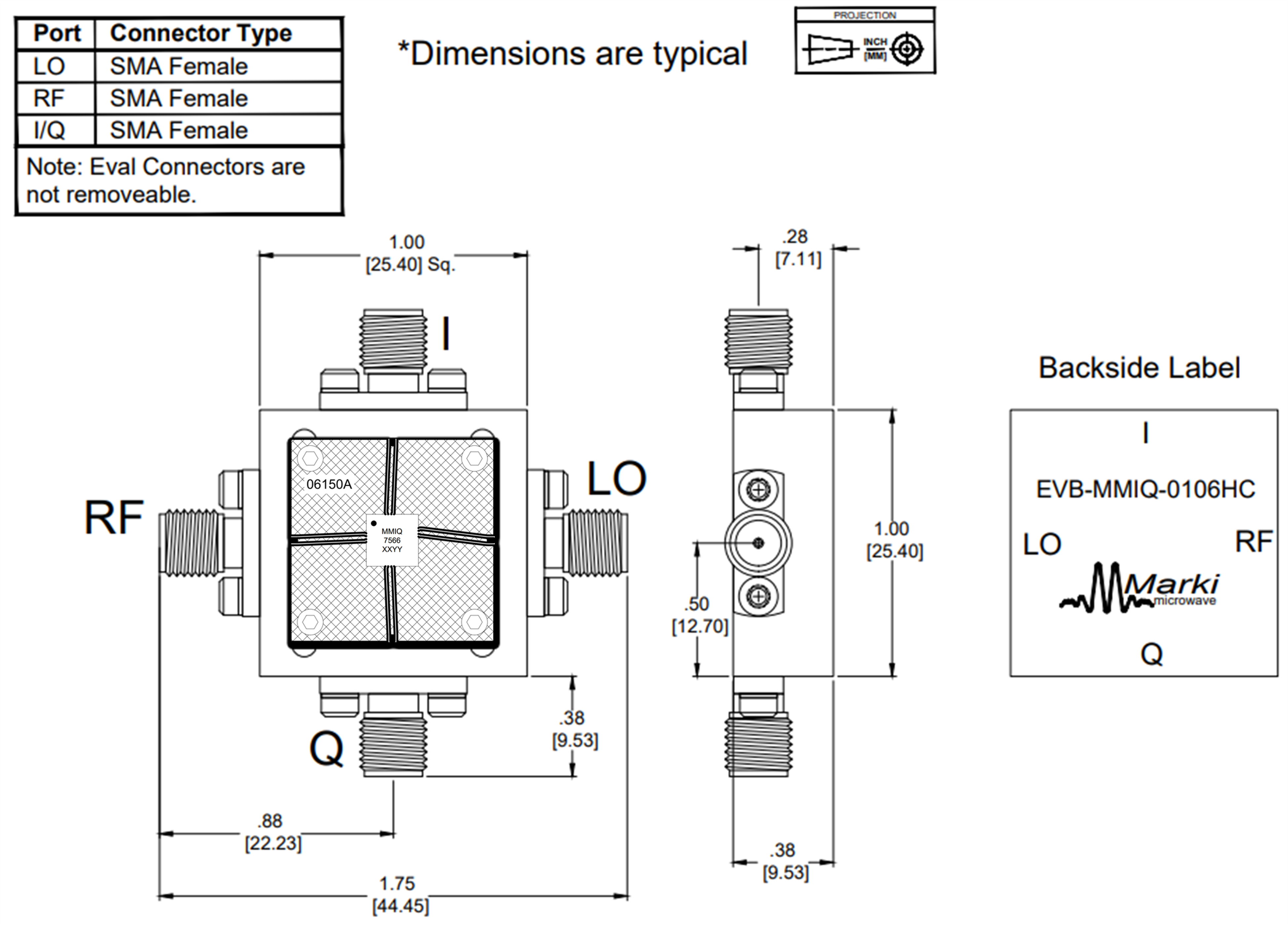
Port Diagram
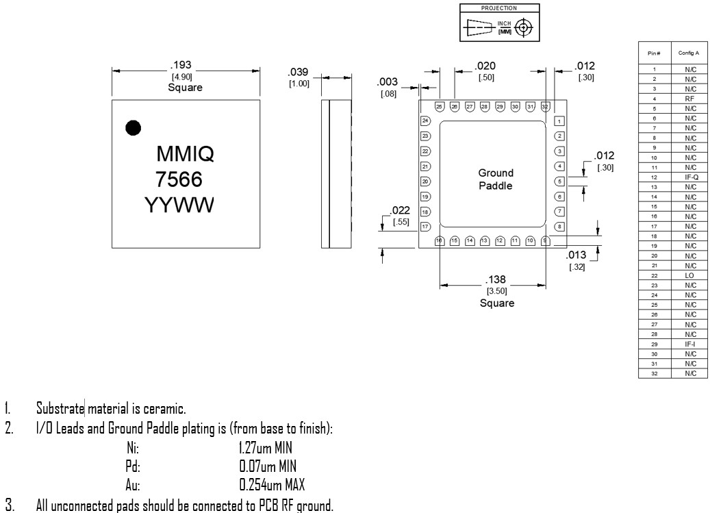
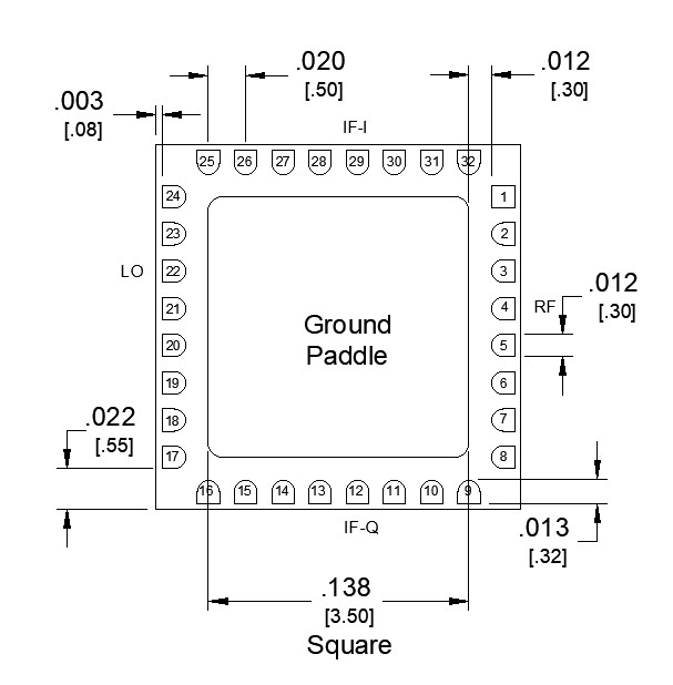
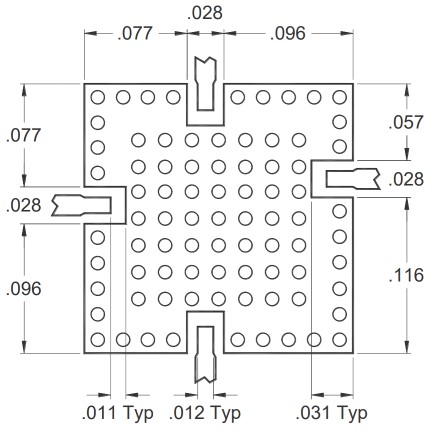
A bottom-up view of the MMIQ-0106HC’s SM package outline drawing is shown below. The mixer may be operated as either a downconverter or an upconverter. Use of the RF or I/Q as the input or output port will depend on the application.
Sales: 408-778-9952 | General: 408-778-4200 | Fax: 408-778-4300
Sales & Customer Support: [email protected]
Tech Support: [email protected]
MMIQ-0106HCSM is a high linearity, passive GaAs MMIC IQ mixer. This is an ultra-broadband mixer spanning 1.5 to 5.5 GHz on the RF and LO ports with an IF from DC to 3 GHz. Up to 33 dB of image rejection is available due to the excellent phase and amplitude balance of its on-chip LO quadrature hybrid. The MMIQ 0106HCSM is available in a 5x5 mm ceramic QFN package. Evaluation boards are available.
|
Parameter |
Typical |
Unit |
|
RF/LO Frequency Range |
1.5 – 5.5 |
GHz |
|
IF Frequency Range |
DC – 3 |
GHz |
|
I+Q Conversion Loss |
8 |
dB |
|
Image Rejection |
33 |
dBc |
|
LO-RF Isolation |
62 |
dB |

| Part Number | Description | Package | Green Status | Product Lifecycle | Export Classification |
|---|---|---|---|---|---|
| MMIQ-0106HCSM-2 | Passive GaAs MMIC IQ Mixer | QFN | REACH RoHS | Released | EAR99 |
| EVB-MMIQ-0106HC | Evaluation Board, Passive GaAs MMIC 1.5 - 5.5 GHz IQ Mixer. | EVB | REACH RoHS | Released | EAR99 |
MMIQ-0106HCSM-2
Passive GaAs MMIC IQ Mixer
| Revision Code | Revision Date | Comment |
|---|---|---|
| - | 2022-06-01 | Datasheet Initial Release |
MMIQ-0106HCSM-2
Passive GaAs MMIC IQ Mixer
A bottom-up view of the MMIQ-0106HC’s SM package outline drawing is shown below. The mixer may be operated as either a downconverter or an upconverter. Use of the RF or I/Q as the input or output port will depend on the application.
| Port | Function | Description | DC Equivalent Circuit |
|---|---|---|---|
| Pin 12 | Q Input / Output | Pin 12 is diode coupled and AC matched to 50Ω over the specified Q port frequency range. |  |
| Pin 22 | LO Input | Pin 22 is DC short and AC matched to 50Ω over the specified RF frequency range. |  |
| Pin 29 | I Input / Output | Pin 29 is diode coupled and AC matched to 50Ω over the specified I port frequency range. |  |
| Pin 4 | RF Input / Output | Pin 4 is DC short and AC matched to 50Ω over the specified RF frequency range. |  |
MMIQ-0106HCSM-2
Passive GaAs MMIC IQ Mixer
The Absolute Maximum Ratings indicate limits beyond which damage may occur to the device. If these limits are exceeded, the device may be inoperable or have a reduced lifetime.
| Parameter | Maximum Rating | Unit |
|---|---|---|
| Maximum Operating Temperature | 100 | °C |
| Maximum Storage Temperature | 125 | °C |
| Minimum Operating Temperature | -55 | °C |
| Minimum Storage Temperature | -65 | °C |
| Pin 22 DC Current | 30 | mA |
| Pin 4 DC Current | 30 | mA |
| Power Handling, at any Port 1 | 26 | dBm |
[1] +26 dBm at +25°C, derated linearly to +23 dBm at +100°C
| Parameter | Details | Rating |
|---|---|---|
| ESD | 250 to < 500 Volts | HBM Class 1A |
| Dimensions | - | 5 x 5 mm |
| Moisture Sensitivity Level | - | MSL 1 |
The Recommended Operating Conditions indicate the limits, inside which the device should be operated, to guarantee the performance given in Electrical Specifications Operating outside these limits may not necessarily cause damage to the device, but the performance may degrade outside the limits of the electrical specifications. For limits, above which damage may occur, see Absolute Maximum Ratings.
| Parameter | Min | Nominal | Max | Unit |
|---|---|---|---|---|
| Ambient Temperature | -55 | 25 | 100 | °C |
| LO Input Power | 16 | 18 | 20 | dBm |
| RF/IF Input Power | - | - | 11 | dBm |
MMIQ-0106HCSM-2
Passive GaAs MMIC IQ Mixer
The electrical specifications apply at TA=+25°C in a 50Ω system. Typical data shown is for a down conversion application with a +18 dBm sine wave LO input. Min and Max limits apply only to our connectorized units and are guaranteed at TA=+25°C. All QFNs are 100% RF tested and visually inspected.
| Parameter | Test Conditions | Minimum Frequency (GHz) | Maximum Frequency (GHz) | Min | Typ | Max | Unit |
|---|---|---|---|---|---|---|---|
| Amplitude Balance 1 | RF/LO = 1.5 – 5.5 GHz | 1.5 | 5.5 | - | 0.3 | - | dB |
| Conversion Loss 2 | RF/LO = 1.5 – 5.5 GHz I = 0.2 - 3 GHz | 1.5 | 5.5 | - | 12.5 | - | dB |
| Conversion Loss 3 | RF/LO = 1.5 – 5.5 GHz Q = 0.2 - 3 GHz | 1.5 | 5.5 | - | 12.5 | - | dB |
| Conversion Loss 4 | RF/LO = 1.5 – 5.5 GHz Q = DC - 0.2 GHz | 1.5 | 5.5 | - | 11 | 14 | dB |
| IF Frequency Range | - | - | - | 0 | - | 3 | GHz |
| Image Rejection 5 | RF/LO = 1.5 – 55. GHz I+Q = DC – 0.2 GHz | 1.5 | 5.5 | - | 33 | - | dBc |
| Input 1 dB Gain Compression Point (P1dB), I | - | - | - | - | 11 | - | dBm |
| Input 1 dB Gain Compression Point (P1dB), Q | - | - | - | - | 11 | - | dBm |
| Input IP3 6 | RF/LO = 1.5 – 5.5 GHz I = DC – 0.2 GHz | 1.5 | 5.5 | - | 22 | - | dBm |
| LO Frequency Range | - | - | - | 1.5 | - | 5.5 | GHz |
| LO-IF Isolation | IF/LO = 1.5 – 5.5 GHz | 1.5 | 5.5 | - | 32 | - | dB |
| LO-RF Isolation | RF/LO = 1.5 – 5.5 GHz | 1.5 | 5.5 | - | 62 | - | dB |
| Noise Figure 7 | RF/LO = 1.5 – 5.5 GHz I = DC – 0.2 GHz | 1.5 | 5.5 | - | 11 | - | dB |
| Noise Figure 8 | RF/LO = 1.5 – 5.5 GHz Q = DC – 0.2 GHz | 1.5 | 5.5 | - | 11 | - | dB |
| Phase Balance | RF/LO = 1.5 – 5.5 GHz | 1.5 | 5.5 | - | 4 | - | ° |
| Q (Port 3) Frequency Range | - | - | - | 0 | - | 3 | GHz |
| RF Frequency Range | - | - | - | 1.5 | - | 5.5 | GHz |
| RF-IF Isolation | RF/IF = 1.5 – 5.5 GHz | 1.5 | 5.5 | - | 43 | - | dB |
| Conversion Loss 9 | RF/LO = 1.5 – 5.5 GHz I = DC - 0.2 GHz | 1.5 | 5.5 | - | 11 | - | dB |
[1] Amplitude and phase balance measured in a down conversion.
[2][3][4][9] Measured as an I/Q down converter (i.e., I and Q powers are not combined)
[5] Image Rejection and Single sideband performance plots are defined by the upper sideband (USB) or lower sideband (LSB) with respect to the LO signal. Plots are defined by which sideband is selected by the external IF quadrature hybrid.
[6] Typical IIP3 is measured with I and Q ports combined with an external quadrature hybrid coupler in a down conversion.
[7][8] Mixer Noise Figure typically measures within 0.5 dB of conversion loss for IF frequencies greater than 5 MHz.
MMIQ-0106HCSM-2
Passive GaAs MMIC IQ Mixer
I output means that the IF output signal is measured at the I port of the mixer and the Q port is loaded. Q output means the IF output signal is measured at the Q port of the mixer while the I port is loaded.


MMIQ-0106HCSM-2
Passive GaAs MMIC IQ Mixer


MMIQ-0106HCSM-2
Passive GaAs MMIC IQ Mixer


MMIQ-0106HCSM-2
Passive GaAs MMIC IQ Mixer


MMIQ-0106HCSM-2
Passive GaAs MMIC IQ Mixer
MMIQ-0106HCSM-2
Passive GaAs MMIC IQ Mixer
Download : Footprint Drawing
MMIQ-0106HCSM-2
Passive GaAs MMIC IQ Mixer