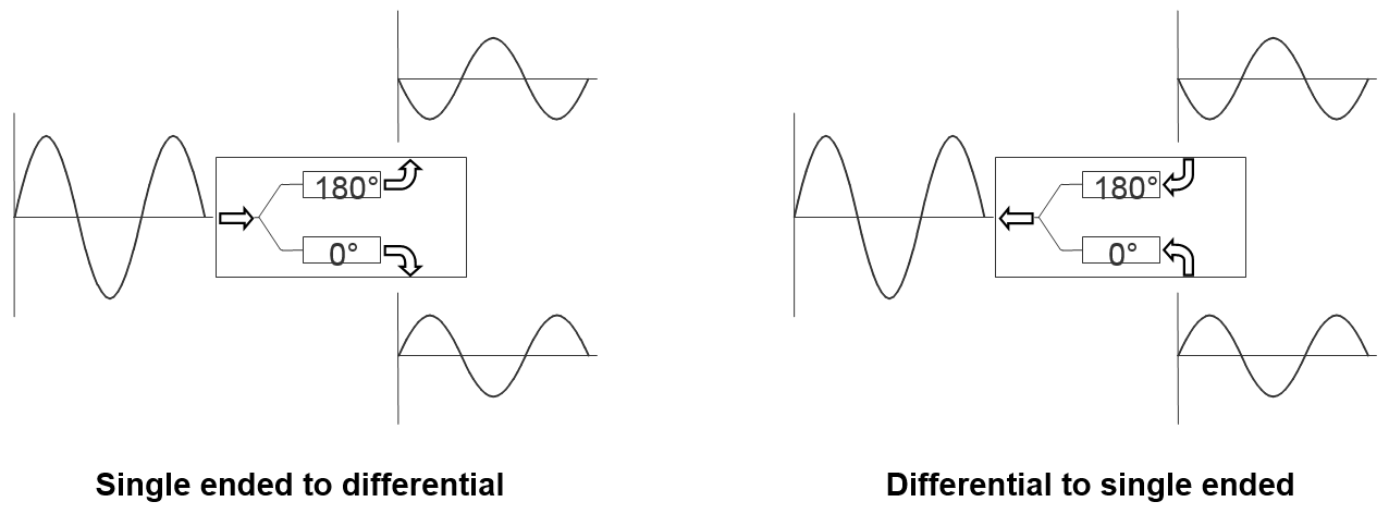
Port Diagram

Sales: 408-778-9952 | General: 408-778-4200 | Fax: 408-778-4300
Sales & Customer Support: [email protected]
Tech Support: [email protected]
The MBAL-0220CSP2 is a GaAs passive MMIC balun featuring a frequency range of 2 to 20 GHz. This balun offers low 1.9 dB insertion loss as a mode converter, excellent balance and 27 dB common mode rejection in a compact 2.5 mm CSP2 chip scale package. The leadfree, RoHS compliant CSP2 package is compatible with standard pick and place assembly. It is an ideal solution to interface into dataconverters for S-K band digital beamforming and other higher order Nyquist sampling applications, clock distribution, and balanced amplifiers.

| Part Number | Description | Package | Packing Size | Green Status | Product Lifecycle | Export Classification |
|---|---|---|---|---|---|---|
| MBAL-0220CSP2 | 2-20 GHz Passive MMIC Chip Scale Package Balun | CSP2 | - | REACH RoHS | Released | EAR99 |
| EVB-MBAL-0220 | Evaluation Board, 2-20 GHz Passive MMIC Chip Scale Package Balun | EVB | - | REACH RoHS | Released | EAR99 |
| MBAL-0220CSP-TR | Tape and Reel, 2-20 GHz Passive MMIC Chip Scale Package Balun | CSP2 | 13" | REACH RoHS | Released | EAR99 |
MBAL-0220CSP2
2-20 GHz Passive MMIC Chip Scale Package Balun
| Revision Code | Revision Date | Comment |
|---|---|---|
| - | 2024-02-28 | Datasheet Initial Release |
| A | 2024-10-15 | Updated ESD information |
| B | 2025-04-28 | Updated Moisture Sensitivity from MSL3 to MSL1 |
MBAL-0220CSP2
2-20 GHz Passive MMIC Chip Scale Package Balun
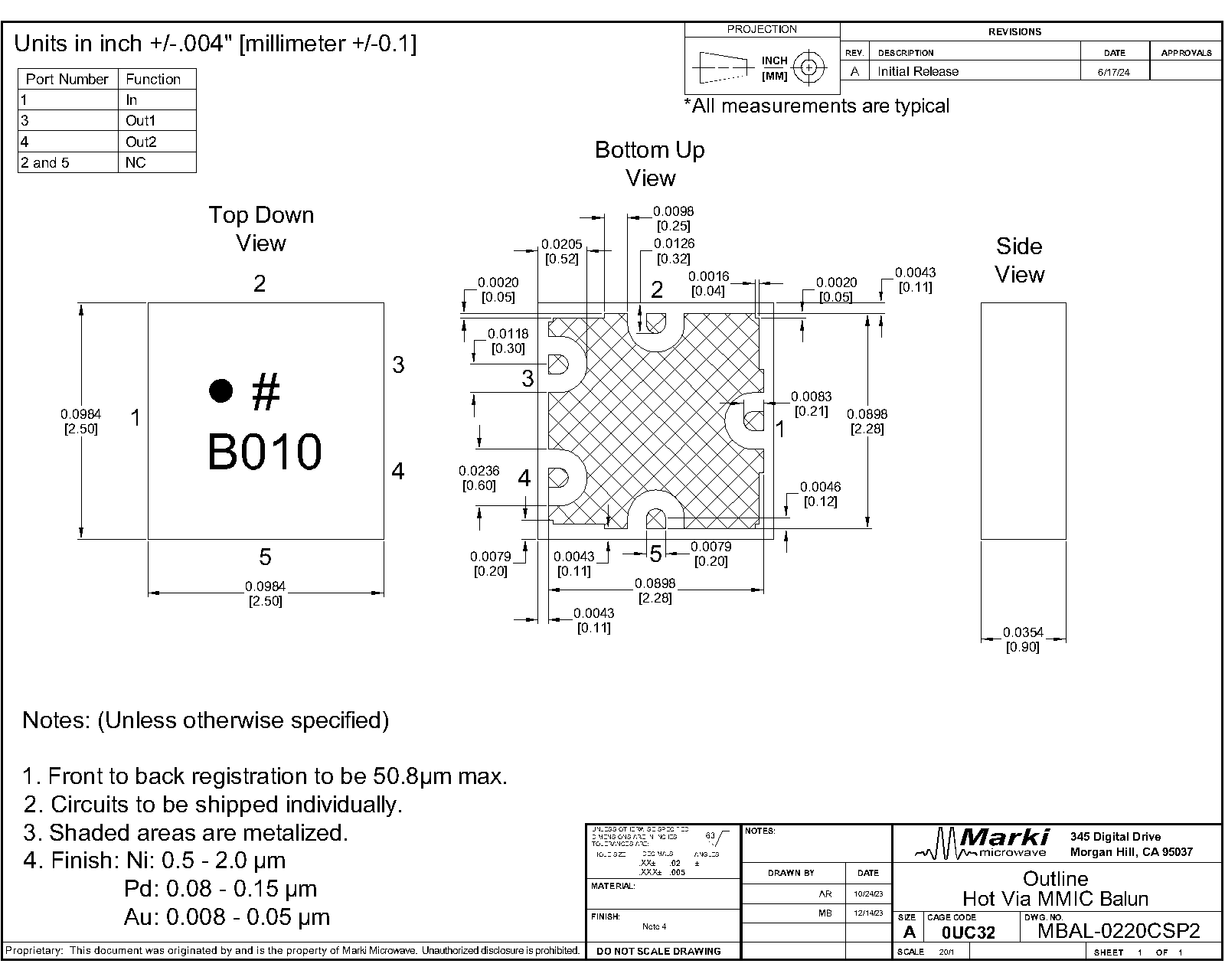
| Port | Function | Description | DC Equivalent Circuit |
|---|---|---|---|
| GND | Ground | Ground pad should be connected to RF/DC ground with low electrical and thermal resistance. |  |
| Pin 1 | Common Port / In (Unbalanced) | The common port is DC open to ground. |  |
| Pin 3 | Out 1 / 0° Port (Balanced) | The 0° port is DC short to ground. |  |
| Pin 4 | Out 2 / 180° Port (Balanced) | The 180° port is DC short to ground. | |
| Pins 2,5 | NC | Pins 2 and 5 are not internally connected. They can be connected to ground for normal operation. | |
MBAL-0220CSP2
2-20 GHz Passive MMIC Chip Scale Package Balun
| Parameter | Maximum Rating | Unit |
|---|---|---|
| Maximum Operating Temperature | 100 | °C |
| Maximum Storage Temperature | 125 | °C |
| Minimum Operating Temperature | -55 | °C |
| Minimum Storage Temperature | -65 | °C |
| RF Power Handling | 36 | dBm |
| Parameter | Details | Rating |
|---|---|---|
| ESD | 250 to < 500 Volts | HBM Class 1A |
| Dimensions | - | 2.50 x 2.50 mm |
| Moisture Sensitivity Level | - | MSL 1 |
MBAL-0220CSP2
2-20 GHz Passive MMIC Chip Scale Package Balun
| Parameter | Test Conditions | Minimum Frequency (GHz) | Maximum Frequency (GHz) | Min | Typ | Max | Unit |
|---|---|---|---|---|---|---|---|
| Output Return Loss | - | 2 | 20 | - | 7 | - | dB |
| Amplitude Balance | - | 2 | 20 | - | 0.3 | 1 | dB |
| Common Mode Rejection | - | 2 | 20 | 20 | 27 | - | dB |
| Common Port Return Loss | - | 2 | 20 | - | 13 | - | dB |
| Impedance | - | 2 | 20 | - | 50 | - | Ω |
| Impedance Ratio | - | - | - | - | 2:1 | - | - |
| Insertion Loss as a Mode Converter | - | 3 | 20 | - | 1.9 | 4 | dB |
| Insertion Loss as a Mode Converter | - | 2 | 3 | - | 1.4 | 6 | dB |
| Isolation | - | 2 | 20 | - | 5 | - | dB |
| Nominal Phase Shift | - | 2 | 20 | - | 180 | - | ° |
| Phase Balance | - | 2 | 20 | - | 3 | 10 | ° |
MBAL-0220CSP2
2-20 GHz Passive MMIC Chip Scale Package Balun
Mixed mode scattering parameters are used to characterize differential circuits. For baluns, this means that the 0° and 180° ports become a single 100Ω differential port and the common port remains the same 50Ω common port. The two-port s-parameters of the balun are then characterized based on differential (d), common mode (c), or single-ended (s) signals. For example: Scs12 is the Common output response given a single ended input.


MBAL-0220CSP2
2-20 GHz Passive MMIC Chip Scale Package Balun


Measured data is de-embedded from fixture using AFR.
MBAL-0220CSP2
2-20 GHz Passive MMIC Chip Scale Package Balun
Download : Outline 2D Drawing Outline 3D Drawing Outline 3D STP
EVB Out- refers to output Out 1
EVB Out+ refers to output Out 2
MBAL-0220CSP2
2-20 GHz Passive MMIC Chip Scale Package Balun
Download : Footprint Drawing

MBAL-0220CSP2
2-20 GHz Passive MMIC Chip Scale Package Balun
| Parameter | Test Conditions | Frequency Range (GHz) | Min | Typ | Max | Unit |
|---|---|---|---|---|---|---|
| Impedance Ratio | - | - | - | 2 | - | - |
MBAL-0220CSP2
2-20 GHz Passive MMIC Chip Scale Package Balun
