Port Diagram
A top-down port diagram of the APM-6848SM is shown below.
OBSOLETE
Sales: 408-778-9952 | General: 408-778-4200 | Fax: 408-778-4300
Sales & Customer Support: [email protected]
Tech Support: [email protected]
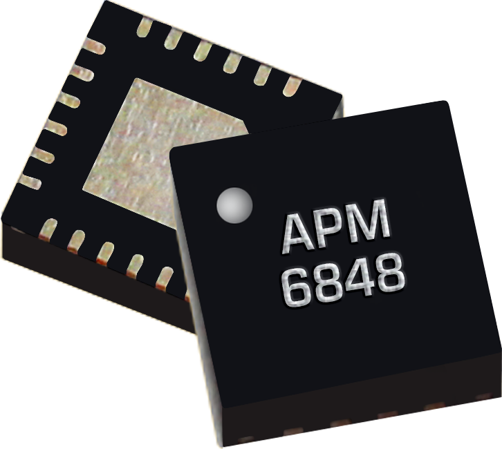
The APM-6848SM is an integrated 2-stage broadband, low phase noise LO driver amplifier designed to provide a saturated +20 dBm output power from a 0-4 dBm input power with low DC power consumption, packaged in a 4mm QFN. This amplifier uses GaAs HBT technology for low phase noise, and is optimized to provide enough power to drive the LO port of an S-diode mixer from 2 GHz to 20 GHz or an H or L diode mixer from 2 GHz to 32 GHz. This amplifier can be operated with a variety of bias conditions including VC=VB=5V for both low power and high power applications.

| Part Number | Description | Package | Green Status | Product Lifecycle | Export Classification |
|---|---|---|---|---|---|
| APM-6848SM | 2-30 GHz Surface Mount Low Phase Noise Amplifier | QFN | REACH RoHS | Obsolete | EAR99 |
| EVAL-APM-6848SM | Evaluation Board, 2-30 GHz Surface Mount Low Phase Noise Amplifier | EVAL | REACH RoHS | Obsolete | EAR99 |
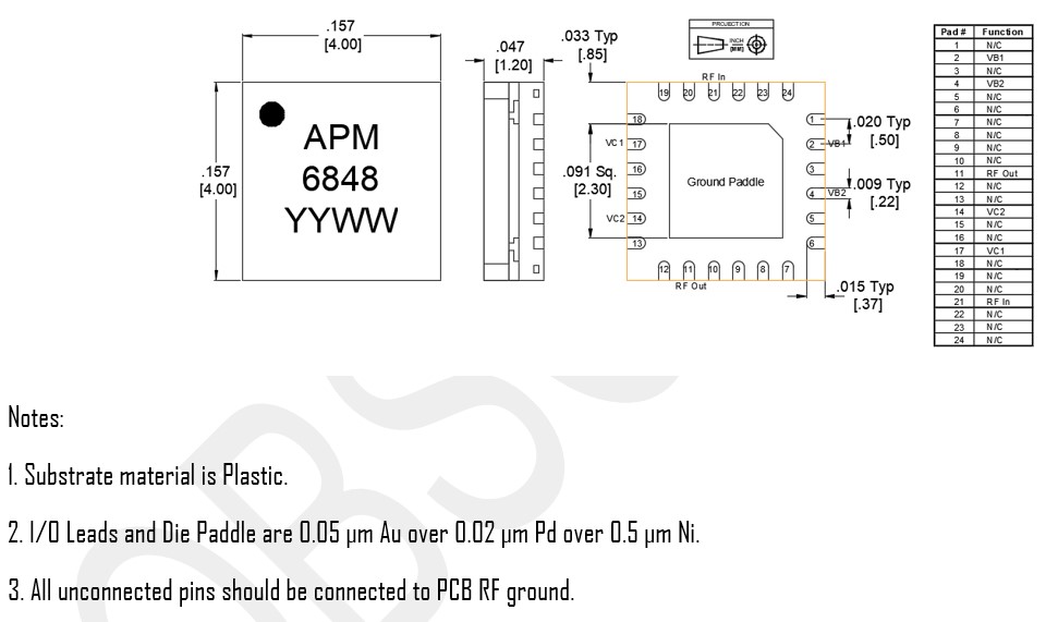
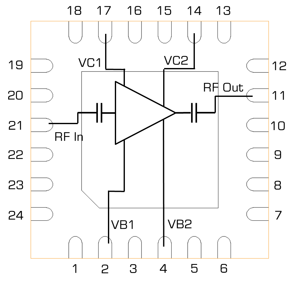
APM-6848SM
2-30 GHz Surface Mount Low Phase Noise Amplifier
| Revision Code | Revision Date | Comment |
|---|---|---|
| - | 2019-12-01 | Datasheet Initial Release |
| A | 2020-05-01 | Updated EVAL drawing and status |
| B | 2020-07-01 | Updated Min small signal gain spec |
| C | 2020-07-01 | Updated Max Operating Temperature |
| D | 2020-11-01 | Updated Thermal Specs and Min Specs, added link to landing pattern |
| E | 2020-12-01 | Adjusted performance plots to adhere to Max input power spec. |
APM-6848SM
2-30 GHz Surface Mount Low Phase Noise Amplifier
A top-down port diagram of the APM-6848SM is shown below.
APM-6848SM
2-30 GHz Surface Mount Low Phase Noise Amplifier
| Port | Function | Description | DC Equivalent Circuit |
|---|---|---|---|
| 11 | RF Output | This is the RF Output port of the amplifier die. It is internally DC blocked and RF matched to 50 Ω. Must have less than 7:1 VSWR when operating with voltage larger than 5V on VC1 or VC2. |  |
| 14 | Collector Supply Port 2 | Pad VC2 is the DC voltage supply pad to the 2nd stage of the amplifier IC. Larger VC voltage will result in larger power consumption and larger power output. See typical performance plots for performance at different bias conditions. |  |
| 17 | Collector Supply Port 1 | Pad VC1 is the DC voltage supply pad for the 1st stage of the amplifier IC. See Typical performance plots for performance at different bias conditions. | |
| 2 | Base Supply Port 1 | Pad VB1 is the DC voltage supply pad for a current mirror which controls the collector current of the 1st stage (Ic1). Larger voltages result in a higher current draw through pad VC1, effectively functioning as a gain control pin for the 1st stage of the amplifier. See typical performance plots for performance at different bias conditions. |  |
| 21 | RF Input | This is the RF Input port of the amplifier die. It is internally DC blocked and RF matched to 50 Ω. | |
| 4 | Base Supply Port 2 | Pad VB2 is the DC voltage supply pad for a current mirror which controls the collector current of the 2nd stage (Ic2). Larger voltages result in a higher current draw through pad VC2, effectively functioning as a gain control pin for the 2nd stage of the amplifier. See typical performance plots for performance at different bias conditions. | |
| GND | Ground | Backside of the IC must be connected to a DC/RF ground with high thermal and electrical conductivity. |  |
APM-6848SM
2-30 GHz Surface Mount Low Phase Noise Amplifier
The Absolute Maximum Ratings indicate limits beyond which damage may occur to the device. If these limits are exceeded, the device may become inoperable or have a reduced lifetime.
| Parameter | Maximum Rating | Unit |
|---|---|---|
| Collector Positive Bias Voltage (VC, VC1, VC2) | 7 | V |
| Current Mirror Positive Bias Current (Ib, Ib1+Ib2) | 8 | mA |
| Current Mirror Positive Bias Voltage (VB, VB1, VB2) | 7 | V |
| Maximum Operating Temperature | 85 | °C |
| Maximum Storage Temperature | 150 | °C |
| Max Junction Temperature for MTTF > 1E6 Hours | 125 | °C |
| Minimum Operating Temperature | -40 | °C |
| Minimum Storage Temperature | -65 | °C |
| Output Load VSWR | 7 | - |
| Positive Bias Current (Ic1) 1 | 90 | mA |
| Positive Bias Current (Ic2) | 90 | mA |
| RF Input Power | 5 | dBm |
| θJC | 53 | ºC/W |
[1] Maximum positive DC collector current into each collector biasing pin.
| Parameter | Details | Rating |
|---|---|---|
| Dimensions | - | 4 x 4 mm |
| Moisture Sensitivity Level | - | MSL 1 |
The Recommended Operating Conditions indicate the limits, inside which the device should be operated, to guarantee the performance given in Electrical Specifications Operating outside these limits may not necessarily cause damage to the device, but the performance may degrade outside the limits of the electrical specifications. For limits, above which damage may occur, see Absolute Maximum Ratings.
| Parameter | Min | Nominal | Max | Unit |
|---|---|---|---|---|
| Ambient Temperature | -40 | 25 | 85 | °C |
| Positive DC Voltage (VC1) | 3 | 5 | 6 | V |
| Positive DC Current (Ic1) | 8 | 21 | 40 | mA |
| Positive DC Voltage (VC2) | 3 | 5 | 6 | V |
| Positive DC Current (Ic2) | 8 | 21 | 40 | mA |
| Positive DC Current Mirror Voltage (VB1) | 3 | 5 | 6 | V |
| Positive DC Current Mirror Current (Ib1) | 0.9 | 2 | 2.6 | mA |
| Positive DC Current Mirror Voltage (VB2) | 3 | 5 | 6 | V |
| Positive DC Current Mirror Voltage (Ib2) | 0.9 | 2 | 2.6 | mA |
Maximum recommended operating current conditions without RF input applied. Please see typical performance plots for relationship between RF input power and DC current draw.
APM-6848SM
2-30 GHz Surface Mount Low Phase Noise Amplifier
The electrical specifications apply at TA=+25°C in a 50Ω system. All Specifications and performance shown with VC1 = VC2 and VB1 = VB2
| Parameter | Test Conditions | Minimum Frequency (GHz) | Maximum Frequency (GHz) | Min | Typ | Max | Unit |
|---|---|---|---|---|---|---|---|
| Current Consumption 1 | 5V/4V | - | - | - | 27 | - | mA |
| Current Consumption 2 | 5V/5V | - | - | - | 43 | - | mA |
| Current Consumption 3 | 5V/6V | - | - | - | 67 | - | mA |
| Current Mirror, Ib | 5V/4V | - | - | - | 2.9 | - | mA |
| Current Mirror, Ib | 5V/5V | - | - | - | 4 | - | mA |
| Current Mirror, Ib | 5V/6V | - | - | - | 5.2 | - | mA |
| Frequency | - | - | - | 2 | - | 30 | GHz |
| Input IP3 | 5V/5V bias, -25 dBm Input Power | 2 | 29 | - | -2 | - | dBm |
| Input Power for Saturation | 5V/5V bias | 2 | 29 | - | 4 | - | dBm |
| Input Return Loss | 5V/5V bias, -25 dBm Input Power | 2 | 20 | - | 14 | - | dB |
| Input Return Loss | 5V/5V bias, -25 dBm Input Power
| 20 | 29 | - | 7 | - | dB |
| Noise Figure | 5V/5V bias, -25 dBm Input Power | 2 | 26.5 | - | 6 | - | dB |
| Output IP3 | 5V/5V bias, -25 dBm Input Power | 2 | 29 | - | 20 | - | dBm |
| Output P1dB | 5V/5V bias | 2 | 20 | - | 19 | - | dBm |
| Output P1dB | 5V/5V bias | 20 | 29 | - | 15 | - | dBm |
| Output Return Loss | 5V/5V bias, -25 dBm Input Power | 20 | 29 | - | 11 | - | dB |
| Output Return Loss | 5V/5V bias, -25 dBm Input Power | 2 | 20 | - | 16 | - | dB |
| Phase Noise @ 10 kHz Offset | 5V/5V bias, +9 dBm Input power, 4 GHz | 2 | 20 | - | -165 | - | dBc/Hz |
| Reverse Isolation | 5V/5V bias, -25 dBm Input Power
| 2 | 29 | - | 62 | - | dB |
| Saturated Output Power | 5V/5V bias, +6 dBm Input Power | 2 | 20 | 18 | 21 | - | dBm |
| Saturated Output Power | 5V/5V bias, +6 dBm Input Power | 20 | 29 | - | 18 | - | dBm |
| Small Signal Gain | 5V/5V bias, -25 dBm Input Power | 20 | 29 | - | 18 | - | dB |
| Small Signal Gain | 5V/5V bias, -25 dBm Input Power
| 2 | 20 | 18 | 22 | - | dB |
[1][2][3] Bias conditions for Ic and Ib tested with no RF input power. See typical performance plots for DC current vs. RF power. Bias conditions presented as VC/VB.
APM-6848SM
2-30 GHz Surface Mount Low Phase Noise Amplifier
Surface mount performance plots are taken in the EVAL-APM-6848 connectorized fixture, and include launch, line, and connector insertion losses.


APM-6848SM
2-30 GHz Surface Mount Low Phase Noise Amplifier


APM-6848SM
2-30 GHz Surface Mount Low Phase Noise Amplifier

APM-6848SM
2-30 GHz Surface Mount Low Phase Noise Amplifier
Fast rise time is desirable for linear T3 mixer operation.


APM-6848SM
2-30 GHz Surface Mount Low Phase Noise Amplifier


APM-6848SM
2-30 GHz Surface Mount Low Phase Noise Amplifier
APM-6848SM
2-30 GHz Surface Mount Low Phase Noise Amplifier
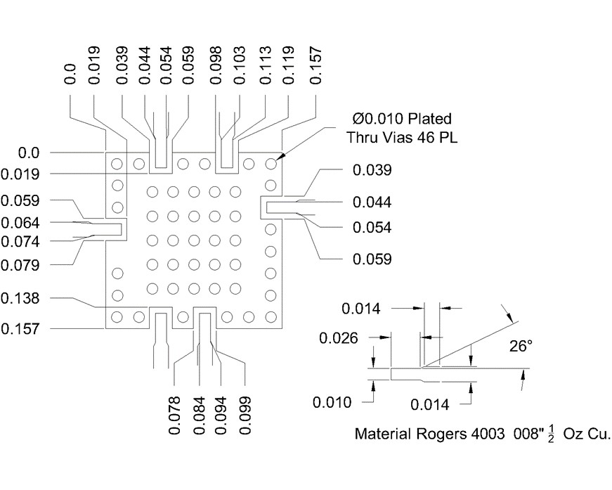
Download : Footprint Drawing