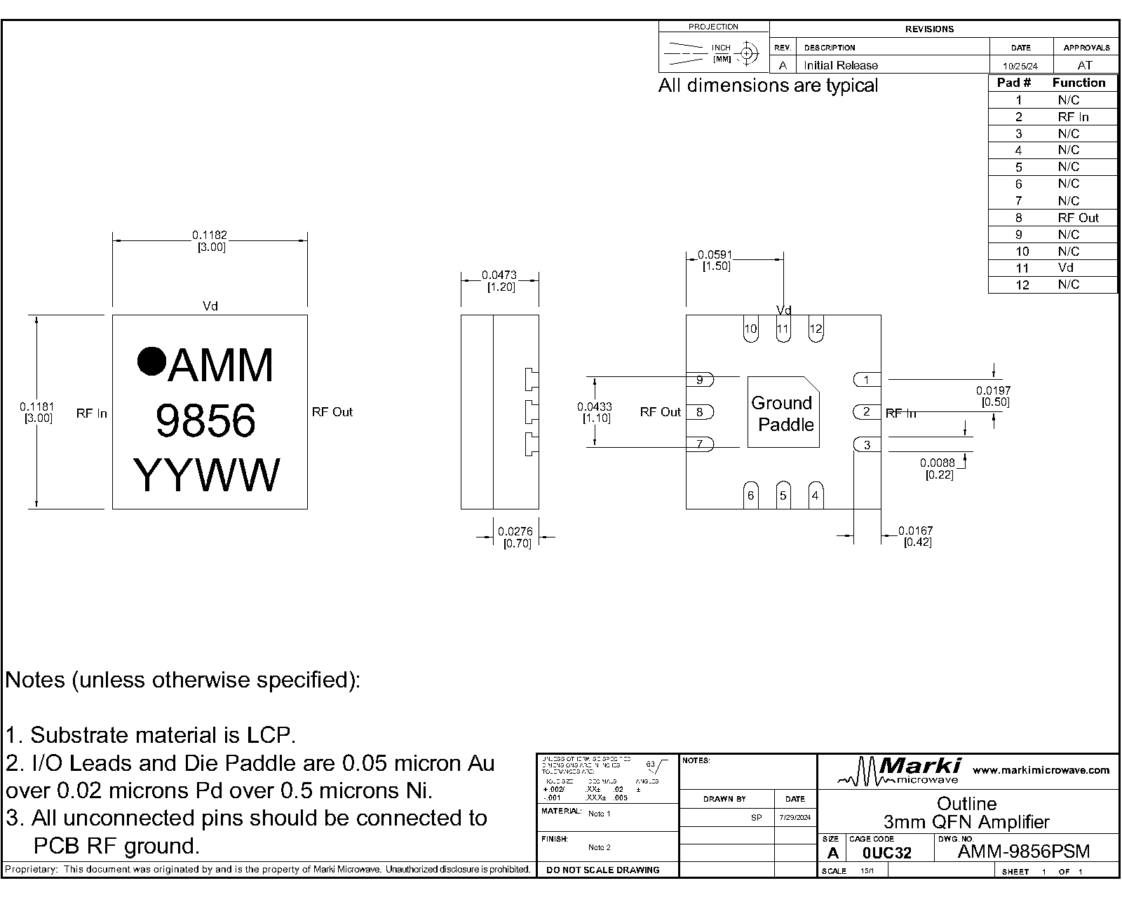
Port Diagram
A port diagram of the AMM-9856PSM’s QFN package is shown below. The diagram is shown as a top down x-ray view.

Sales: 408-778-9952 | General: 408-778-4200 | Fax: 408-778-4300
Sales & Customer Support: [email protected]
Tech Support: [email protected]
The AMM-9856PSM is a surface-mount amplifier suitable for use as a single tone driver or general-purpose gain block. It can drive an L diode mixer up to 40 GHz or an H diode mixer up to 20 GHz. This amplifier also is optimized for excellent gain flatness in-band and high IP3/IP2 performance. The AMM-9856PSM is packaged in a compact 3mm QFN for surface mount integration onto printed circuit boards

| Part Number | Description | Package | Green Status | Product Lifecycle | Export Classification |
|---|---|---|---|---|---|
| AMM-9856PSM | DC-40 GHz GaAs Surface Mount Driver Amplifier | QFN | REACH RoHS | Released | 3A001.b.2.d |
| EVB-AMM-9856P-1 | Evaluation Board, DC-40GHz GaAs Surface Mount Driver Amplifier | EVB | RoHS | Released | EAR99 |
AMM-9856PSM
DC-40 GHz GaAs Surface Mount Driver Amplifier
| Revision Code | Revision Date | Comment |
|---|---|---|
| - | 2024-10-09 | Initial Release |
| A | 2026-02-13 | MTTF Table Added. |
AMM-9856PSM
DC-40 GHz GaAs Surface Mount Driver Amplifier
A port diagram of the AMM-9856PSM’s QFN package is shown below. The diagram is shown as a top down x-ray view.
| Port | Function | Description | DC Equivalent Circuit |
|---|---|---|---|
| GND | Ground | Ground paddle and non-connected pins must be connected to a DC/RF ground potential with high thermal and electrical conductivity, and low inductance. |  |
| Pin 11 | Vd | Pin 11 is the DC bias supply for the amplifier. This pin should be connected to the same supply voltage being used to supply the pin 8 "RF Out / Vd" bias-tee. |  |
| Pin 2 | RF In / Vg | Pin 2 is the RF input of the amplifier and also provides DC bias to the amplifier. This input in internally RF matched to 50 Ohms and requires a bias-tee to a negative DC bias voltage. The bias voltage applied to this pin directly controls the drain current (Id into pin 8) of the amplifier. As the voltage on this pin becomes more negative, drain current decreases. Voltage should be applied to pin 2 before pin 11 "Vd" and pin 8 "RF Out/Vd". See the section on Sequencing Requirements for more details. Current Ig will flow out of this port. The -Vg supply should be capable of sinking current up to 30mA. |  |
| Pin 8 | RF Out / Vd | Pin 8 is the RF output and primary DC power supply of the amplifier. This pin is internally RF matched to 50 ohms and requires an external bias-tee connected to a positive DC supply voltage. Voltage should be applied to pin 2 "RF In/Vg" before applying voltage to pin 8 and pin 11. See the section on Sequencing Requirements for more details. | |
| Pins 1,3,4,5,6,7,9,10,12 | Non-connect (NC) | These pins are not internally connected to the amplifier die. It is recommended to connect these pins to ground to provide RF isolation and mechanical stability. See the recommended landing pattern for details. Datasheet performance was measured with these pins connected to GND. | - |
AMM-9856PSM
DC-40 GHz GaAs Surface Mount Driver Amplifier
The Absolute Maximum Ratings indicate limits beyond which damage may occur to the device. If these limits are exceeded, the device may be inoperable or have a reduced lifetime. This amplifier is designed and characterized in a 50Ω system, and operation in a reflective environment can cause performance degradation.
| Parameter | Maximum Rating | Unit |
|---|---|---|
| Maximum Drain-to-Gate Voltage Differential (Vd-Vg) | 6.7 | V |
| Maximum Operating Temperature | 85 | °C |
| Maximum Storage Temperature | 150 | °C |
| Max Junction Temperature for MTTF > 1E6 hours | 175 | °C |
| Minimum Operating Temperature | -40 | °C |
| Minimum Storage Temperature | -65 | °C |
| Negative Bias Voltage (Pin 2) | -2 | V |
| Positive Drain Supply Current (with RF Input) | 80 | mA |
| Positive Drain Supply Voltage (Pin 8, 11) | 8 | V |
| RF Input Power | 10 | dBm |
| Thermal Resistance, θJC | 120 | ºC/W |
| T (°C) | λ (TIF) | MTTF (hr) | MTTF (yr) |
|---|---|---|---|
| 105 | 2,441.45 | 4.10E+05 | 47 |
| 85 | 310.48 | 3.22E+06 | 368 |
| 55 | 8.79 | 1.14E+08 | 12,992 |
| 25 | 0.12 | 8.24E+09 | 941,063 |
| Parameter | Details | Rating |
|---|---|---|
| Dimensions | - | 3 x 3 mm |
| Moisture Sensitivity Level | - | MSL 1 |
The Recommended Operating Conditions indicate the limits, inside which the device should be operated, to guarantee the performance given in Electrical Specifications. Operating outside these limits may not necessarily cause damage to the device, but the performance may degrade outside the limits of the Electrical Specifications. For limits, above which damage may occur, see Absolute Maximum Ratings .
| Parameter | Min | Nominal | Max | Unit |
|---|---|---|---|---|
| Ambient Temperature | -40 | 25 | 85 | °C |
| Power Supply DC Current | 48 | 61 | 61 | mA |
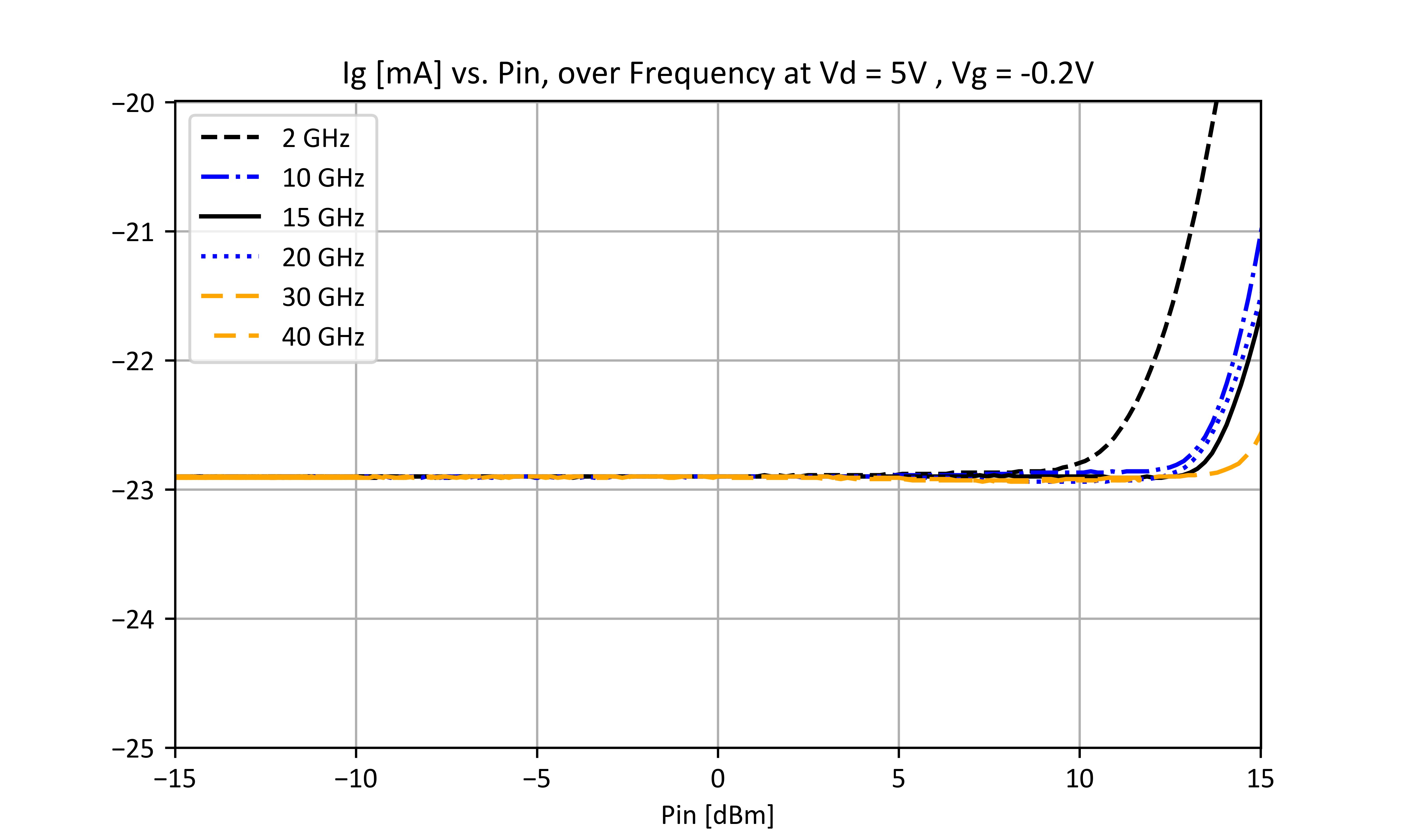
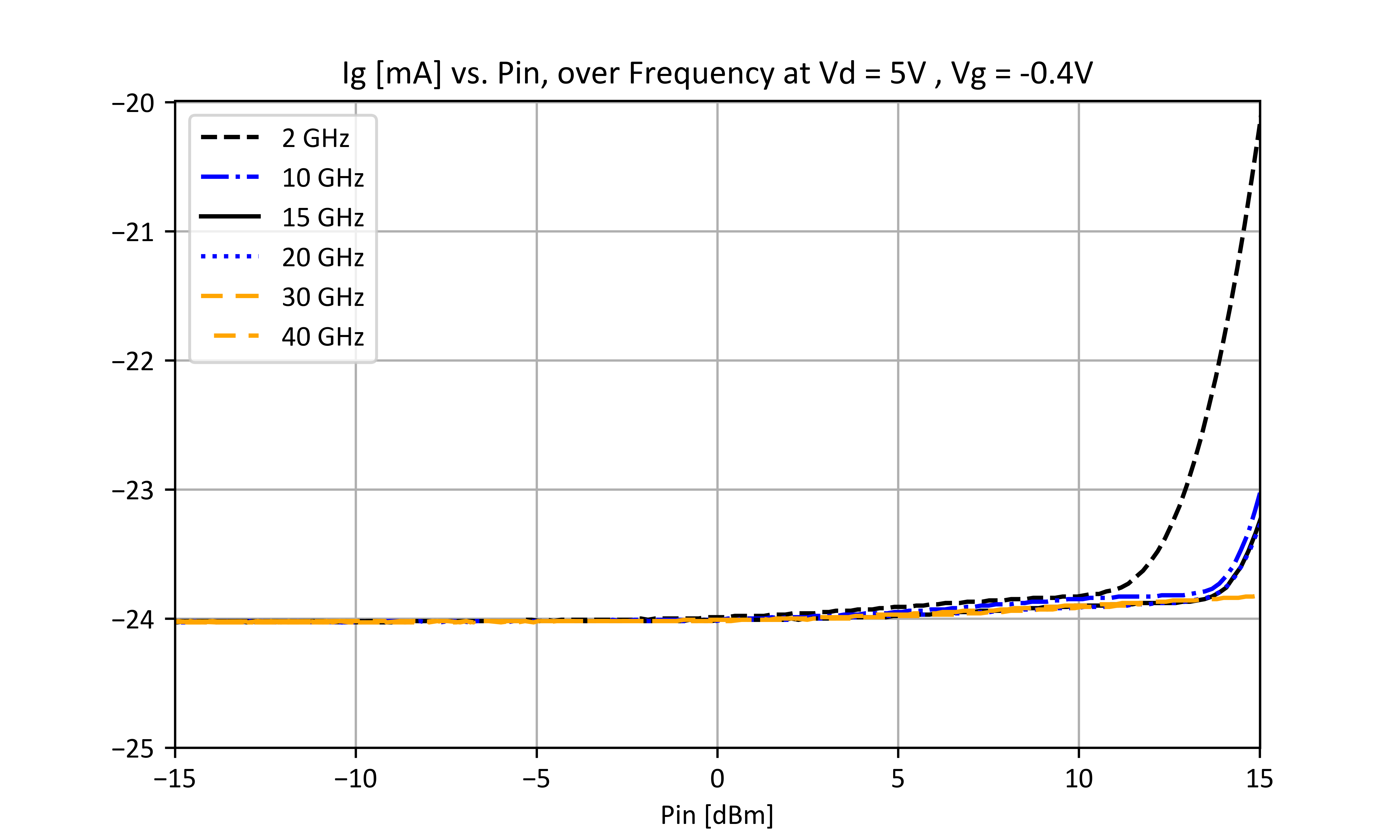
| Gate Bias DC Voltage | -0.4 | -0.2 | -0.2 | V |
| Power Supply DC Voltage | 5 | 5 | 5 | V |
AMM-9856PSM
DC-40 GHz GaAs Surface Mount Driver Amplifier
The electrical specifications apply at TA=+25°C in a 50Ω system. QFNs are 100% RF tested.
| Parameter | Test Conditions | Minimum Frequency (GHz) | Maximum Frequency (GHz) | Min | Typ | Max | Unit |
|---|---|---|---|---|---|---|---|
| Saturated Output Power | - | 2 | 20 | - | 15 | - | dBm |
| Saturated Output Power | - | 2 | 24 | - | 12 | - | dBm |
| Gate Current, Ig 1 | 5V/-0.2V bias | - | - | - | -24 | - | mA |
| Noise Figure | 5V/-0.2V bias, -20 dBm Input Power | 38 | 40 | - | 5.5 | - | dB |
| Output IP3 | 5V/-0.2V bias, -20 dBm Input Power | 30 | 40 | - | 22 | - | dBm |
| Output P1dB | 5V/-0.2V bias | 20 | 40 | - | 10.5 | - | dBm |
| Current Consumption 2 | 5V/-0.2V bias | - | - | - | 61 | - | mA |
| Input Return Loss | 5V/-0.2V bias, -20 dBm Input Power | 0 | 40 | - | 10 | - | dB |
| Noise Figure | 5V/-0.2V bias, -20 dBm Input Power | 0 | 38 | - | 3.8 | - | dB |
| Output IP3 | 5V/-0.2V bias, -20 dBm Input Power | 0 | 30 | - | 25 | - | dBm |
| Output P1dB | 5V/-0.2V bias | 0 | 20 | - | 14 | - | dBm |
| Output Return Loss | 5V/-0.2V bias, -20 dBm Input Power | 0 | 40 | - | 14 | - | dB |
| Reverse Isolation | 5V/-0.2V bias, -20 dBm Input Power | 0 | 40 | - | 15 | - | dB |
| Small Signal Gain | 5V/-0.2V bias, -20 dBm Input Power | 0 | 40 | - | 10 | - | dB |
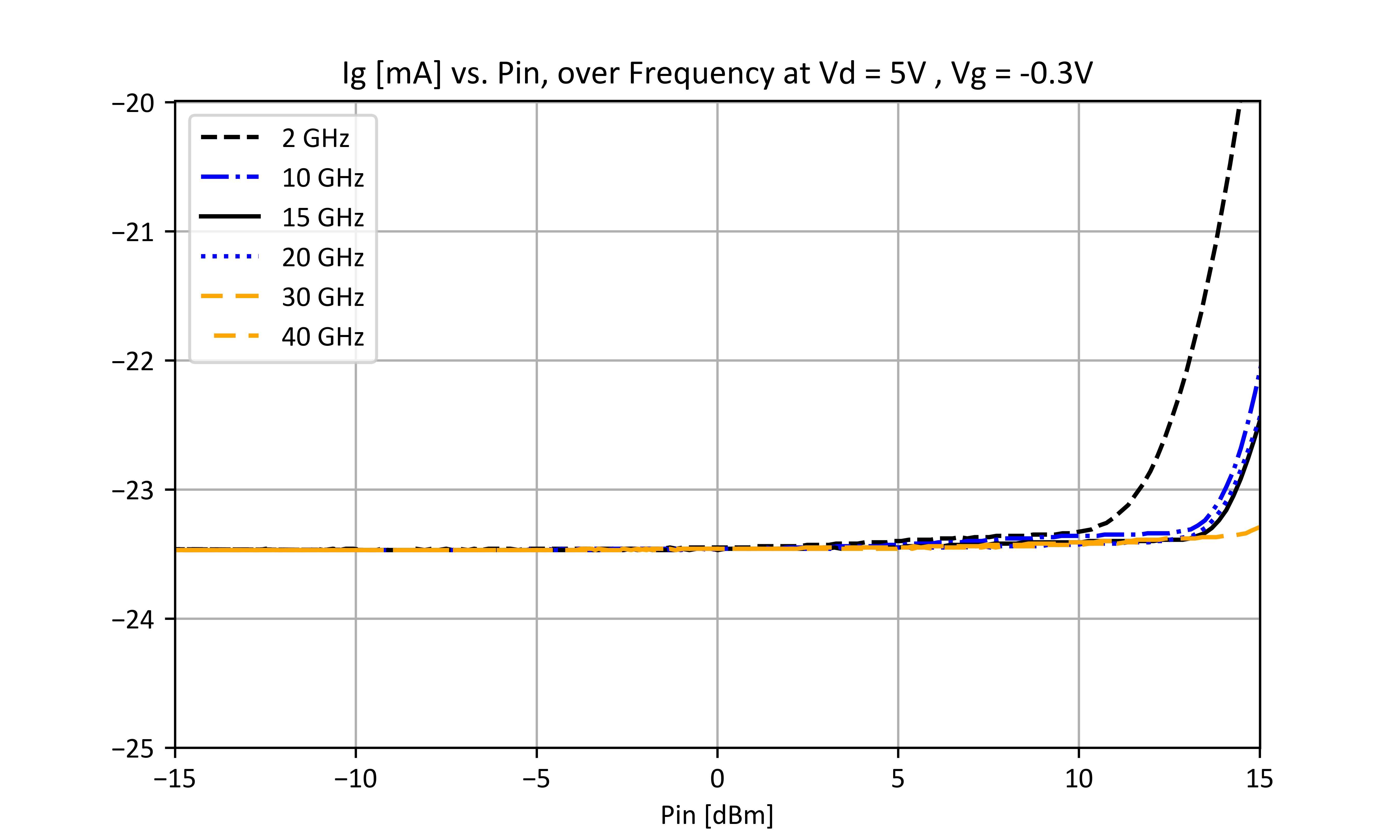
[1] Gate current Ig is shown as a negative value representing it's direction of flow out of Pin 2 when -Vg is applied.
[2] Bias conditions for Id tested with no RF input power. Bias conditions presented as Vd/Vg.
AMM-9856PSM
DC-40 GHz GaAs Surface Mount Driver Amplifier
Measurement data de-embedded using standard evaluation board and external wideband test equipment bias tees.
%20vs.%20Frequency,%20over%20Bias.png)
%20vs.%20Frequency,%20over%20Bias.png)
%20vs.%20Frequency,%20over%20Bias.png)
%20vs.%20Frequency,%20over%20Bias.png)
%20vs.%20Frequency,%20over%20Bias.png)
%20vs.%20Frequency,%20over%20Bias.png)
%20vs.%20Frequency,%20over%20Bias.png)
%20vs.%20Frequency,%20over%20Bias.png)
AMM-9856PSM
DC-40 GHz GaAs Surface Mount Driver Amplifier
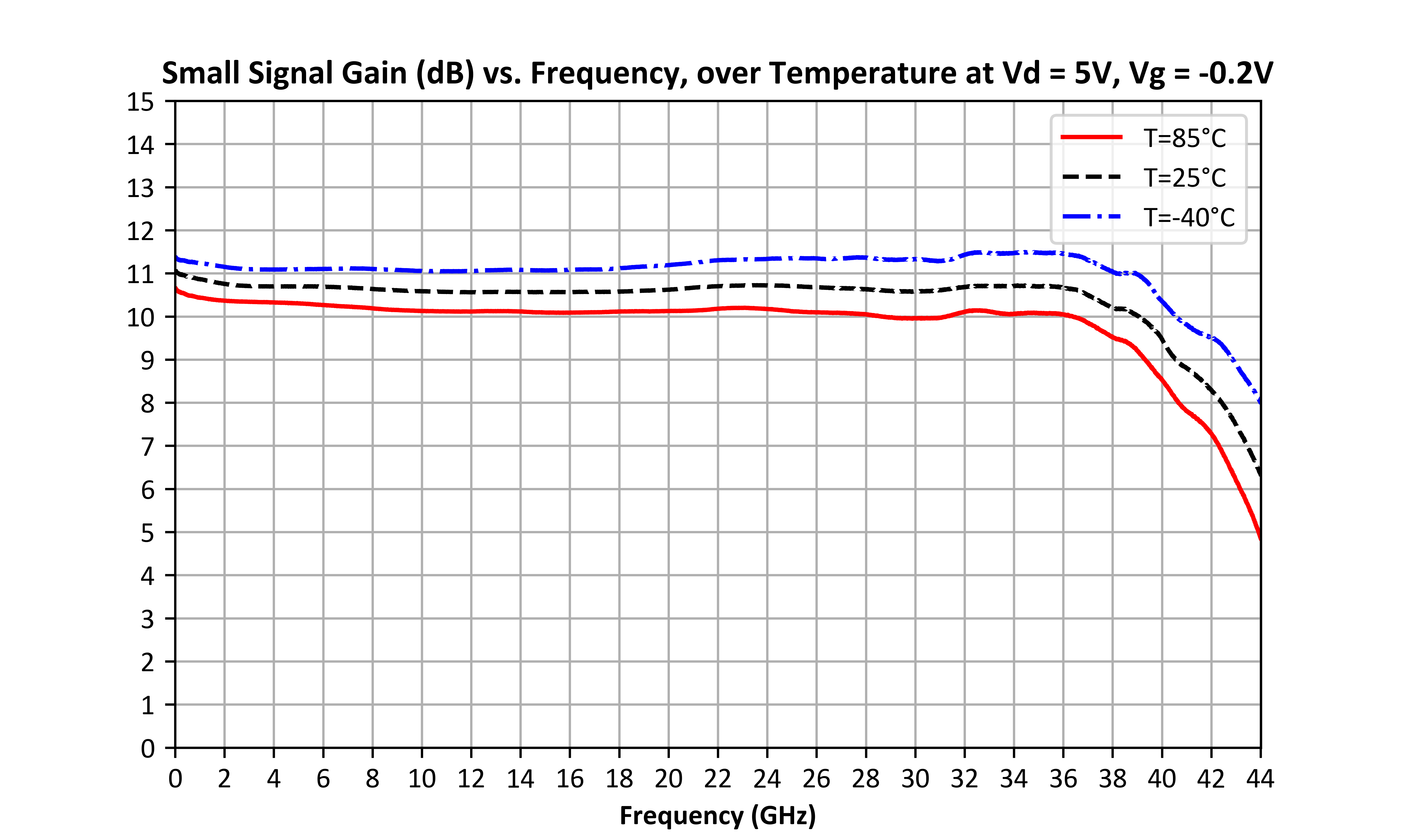
%20vs.%20Frequency,%20over%20Temperature%20at%20Vd%20=%205V,%20Vg%20=%20-0.2V.png)
AMM-9856PSM
DC-40 GHz GaAs Surface Mount Driver Amplifier
%20vs.%20Pin,%20over%20Frequency%20at%20Vd%20=%205V%20,%20Vg%20=%20-0.2V.png)
%20vs.%20Pin,%20over%20Frequency%20at%20Vd%20=%205V%20,%20Vg%20=%20-0.3V.png)
%20vs.%20Pin,%20over%20Frequency%20at%20Vd%20=%205V%20,%20Vg%20=%20-0.4V.png)
%20vs.%20Pin,%20over%20Frequency%20at%20Vd%20=%205V%20,%20Vg%20=%20-0.2V.png)
%20vs.%20Pin,%20over%20Frequency%20at%20Vd%20=%205V%20,%20Vg%20=%20-0.3V.png)
AMM-9856PSM
DC-40 GHz GaAs Surface Mount Driver Amplifier
%20vs.%20Pin,%20over%20Frequency%20at%20Vd%20=%205V%20,%20Vg%20=%20-0.4V.png)
%20vs.%20Pin,%20over%20Frequency%20at%20Vd%20=%205V%20,%20Vg%20=%20-0.2V.png)
%20vs.%20Pin,%20over%20Frequency%20at%20Vd%20=%205V%20,%20Vg%20=%20-0.3V.png)
%20vs.%20Pin,%20over%20Frequency%20at%20Vd%20=%205V%20,%20Vg%20=%20-0.4V.png)
AMM-9856PSM
DC-40 GHz GaAs Surface Mount Driver Amplifier

AMM-9856PSM
DC-40 GHz GaAs Surface Mount Driver Amplifier
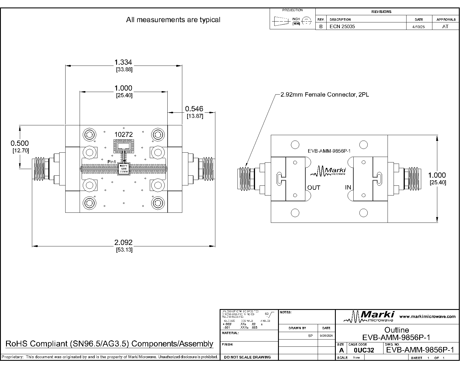
Download : Outline 2D Drawing
Notes (unless otherwise specified):
1. Substrate material is LCP.
2. I/O Leads and Die Paddle are 0.05 micron Au over 0.02 microns Pd over 0.5 microns Ni.
3. All unconnected pins should be connected to
PCB RF ground.
AMM-9856PSM
DC-40 GHz GaAs Surface Mount Driver Amplifier
Download : Footprint Drawing

AMM-9856PSM
DC-40 GHz GaAs Surface Mount Driver Amplifier