Port Diagram
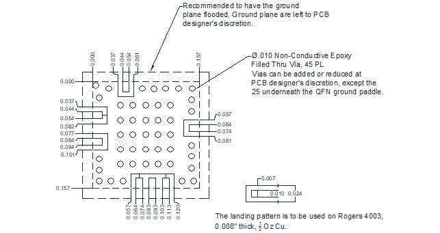
A port diagram of the AMM-7473PSM QFN package is shown below (X-ray view from the top).

Sales: 408-778-9952 | General: 408-778-4200 | Fax: 408-778-4300
Sales & Customer Support: [email protected]
Tech Support: [email protected]
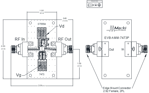
The AMM-7473PSM is a high-linearity, low noise distributed amplifier that can provide +25 dBm output power across its 400 MHz to 27 GHz band and features excellent gain flatness. The AMM-7473PSM can serve either as a linear signal amplifier, or as a saturated driver amplifier for H- or S-diode mixers. Additionally, the AMM-7473PSM incorporates an internal choke inductor which eliminates the need for an external bias tee.


| Part Number | Description | Package | Green Status | Product Lifecycle | Export Classification |
|---|---|---|---|---|---|
| AMM-7473PSM | 0.4 - 27 GHz Surface Mount Amplifier | QFN | REACH RoHS | Released | EAR99 |
| EVB-AMM-7473P | Evaluation Board, 0.4 - 27 GHz Surface Mount Amplifier | EVB | REACH RoHS | Released | EAR99 |
AMM-7473PSM
0.4 - 27 GHz Surface Mount Amplifier
| Revision Code | Revision Date | Comment |
|---|---|---|
| - | 2022-08-01 | Initial Release |
| A | 2025-02-27 | Included ESD rating |
| B | 2026-02-13 | MTTF Table Added. |
AMM-7473PSM
0.4 - 27 GHz Surface Mount Amplifier
A port diagram of the AMM-7473PSM QFN package is shown below (X-ray view from the top).
AMM-7473PSM
0.4 - 27 GHz Surface Mount Amplifier
| Port | Function | Description | DC Equivalent Circuit |
|---|---|---|---|
| 10 | Vg | Pin 10 provides a required negative bias which controls the power supply currents to the amplifier. More negative voltages decrease supply current. Apply gate bias voltage Vg before applying drain power supply. |  |
| 11 | CAP 3 | Pin 11 is connected to internal bias circuitry and should be AC grounded through an off-chip bypass capacitor. The value should be at least 100 nF. This pin should not be directly connected to ground. |  |
| 1,3, 5-8, 12-15, 17-22, 24, Paddle | Ground | These pins should be connected to ground. Package ground paddle must be connected to a DC/RF ground potential with high thermal and electrical conductivity. |  |
| 16 | RF Output | Pin 16 is the RF Output port of the amplifier. It is DC coupled, and RF matched to 50 Ω. An external DC blocking capacitor is required. |  |
| 2 | Cap 1 | Pin 2 allows the user to attach additional off chip bypass capacitance to provide adequate low frequency AC grounding termination to the input matching network. The value should be at least 100 nF. |  |
| 23 | Vd | Pin 23 provides the main power supply for the amplifier. Apply gate bias voltage Vg before applying drain power supply. |  |
| 4 | RF Input | Pin 4 is the RF Input port of the amplifier die. It is internally DC blocked and RF matched to 50 Ω. RF input pad is GSG with 150 µm pitch. |  |
| 9 | Cap 2 | Pin 9 is connected to internal bias circuitry and should be AC grounded through an off-chip bypass capacitor. The value should be at least 100 nF. This pin should not be directly connected to ground. |  |
AMM-7473PSM
0.4 - 27 GHz Surface Mount Amplifier
The Absolute Maximum Ratings indicate limits beyond which damage may occur to the device. If any one of these limits are exceeded, the device may become inoperable or have a reduced lifetime.
| Parameter | Maximum Rating | Unit |
|---|---|---|
| Drain Current (RF Applied) | 550 | mA |
| Drain Supply Voltage (Vd) | 10 | V |
| Gate Voltage (Vg) | 0.5 | V |
| Maximum Operating Temperature for MTTF > 1E6 hours | 85 | °C |
| Maximum Storage Temperature | 150 | °C |
| Max Junction Temperature for MTTF > 1E6 Hours | 175 | °C |
| Max Power Dissipation for MTTF of 1E6 hours at 85˚C Baseplate Temperature | 3.9 | W |
| Minimum Operating Temperature for MTTF > 1E6 hours | -55 | °C |
| Minimum Storage Temperature | -65 | °C |
| RF Input Power | 18 | dBm |
| θ_Jc, Junction to Case Thermal Resistance | 23 | ºC/W |
| T (°C) | λ (TIF) | MTTF (hr) | MTTF (yr) |
|---|---|---|---|
| 105 | 2,441.45 | 4.10E+05 | 47 |
| 85 | 310.48 | 3.22E+06 | 368 |
| 55 | 8.79 | 1.14E+08 | 12,992 |
| 25 | 0.12 | 8.24E+09 | 941,063 |
| Parameter | Details | Rating |
|---|---|---|
| ESD | 125 to < 250 Volts | HBM Class 0B |
| Weight | Package name: QFN | 0.05g |
| Dimensions | - | 4 x 4 mm |
| Moisture Sensitivity Level | - | MSL 1 |
AMM-7473PSM
0.4 - 27 GHz Surface Mount Amplifier
Unless otherwise specified, electrical specifications apply at TA=+25°C, Vd = 7 V, Idq=150 mA (where Idq is the drain current with no RF applied), Vg set as required to achieve Idq = 150 mA in a 50 Ω system.
| Parameter | Test Conditions | Minimum Frequency (GHz) | Maximum Frequency (GHz) | Min | Typ | Max | Unit |
|---|---|---|---|---|---|---|---|
| Output P1dB | Vd =7 V, Vg set to achieve Idq = 150 mA | 0.4 | 20 | - | 22 | - | dBm |
| Current Consumption | Vd = 7 V, Vg = -0.65 V, no RF input applied | - | - | - | 150 | - | mA |
| Input IP3 | Vd = 7 V, Vg set to achieve Idq = 150 mA, Pin = -15 dBm per tone, 10 MHz tone spacing | 0.4 | 27 | - | 18 | - | dBm |
| Input Power for Saturation | Vd = 7 V, Vg set to achieve Idq = 150 mA | 0.4 | 27 | - | 11 | - | dBm |
| Input Return Loss | Vd = 7 V, Vg set to achieve Idq = 150 mA, Pin = -20 dBm | 0.4 | 27 | 8 | - | - | dB |
| Noise Figure | Vd = 7 V, Vg set to achieve Idq = 150 mA, Pin = -20 dBm | 2 | 5 | - | 2.9 | - | dB |
| Noise Figure | Vd = 7 V, Vg set to achieve Idq = 150 mA, Pin = -20 dBm | 15 | 27 | - | 3.6 | - | dB |
| Noise Figure | Vd = 7 V, Vg set to achieve Idq = 150 mA, Pin = -20 dBm | 5 | 15 | - | 1.8 | - | dB |
| Output IP3 | Vd = 7 V, Vg set to achieve Idq = 150 mA, Pin = -15 dBm per tone, 10 MHz tone spacing | 0.4 | 27 | - | 34 | - | dBm |
| Output Return Loss | Vd = 7 V, Vg set to achieve Idq = 150 mA, Pin = -20 dBm | 0.4 | 27 | 8 | - | - | dB |
| Reverse Isolation | Vd = 7 V, Vg set to achieve Idq = 150 mA, Pin = -20 dBm | 0.4 | 27 | - | 40 | - | dB |
| Saturated Output Power | Vd = 7 V, Vg set to achieve Idq = 150 mA, Pin = +15 dBm | 0.4 | 27 | 23 | 25 | - | dBm |
| Small Signal Gain | Vd = 7 V, Vg set to achieve Idq = 150 mA, Pin = -20 dBm | 0.4 | 20 | 14 | 17 | - | dB |
AMM-7473PSM
0.4 - 27 GHz Surface Mount Amplifier


AMM-7473PSM
0.4 - 27 GHz Surface Mount Amplifier


AMM-7473PSM
0.4 - 27 GHz Surface Mount Amplifier

AMM-7473PSM
0.4 - 27 GHz Surface Mount Amplifier
AMM-7473PSM
0.4 - 27 GHz Surface Mount Amplifier
AMM-7473PSM
0.4 - 27 GHz Surface Mount Amplifier