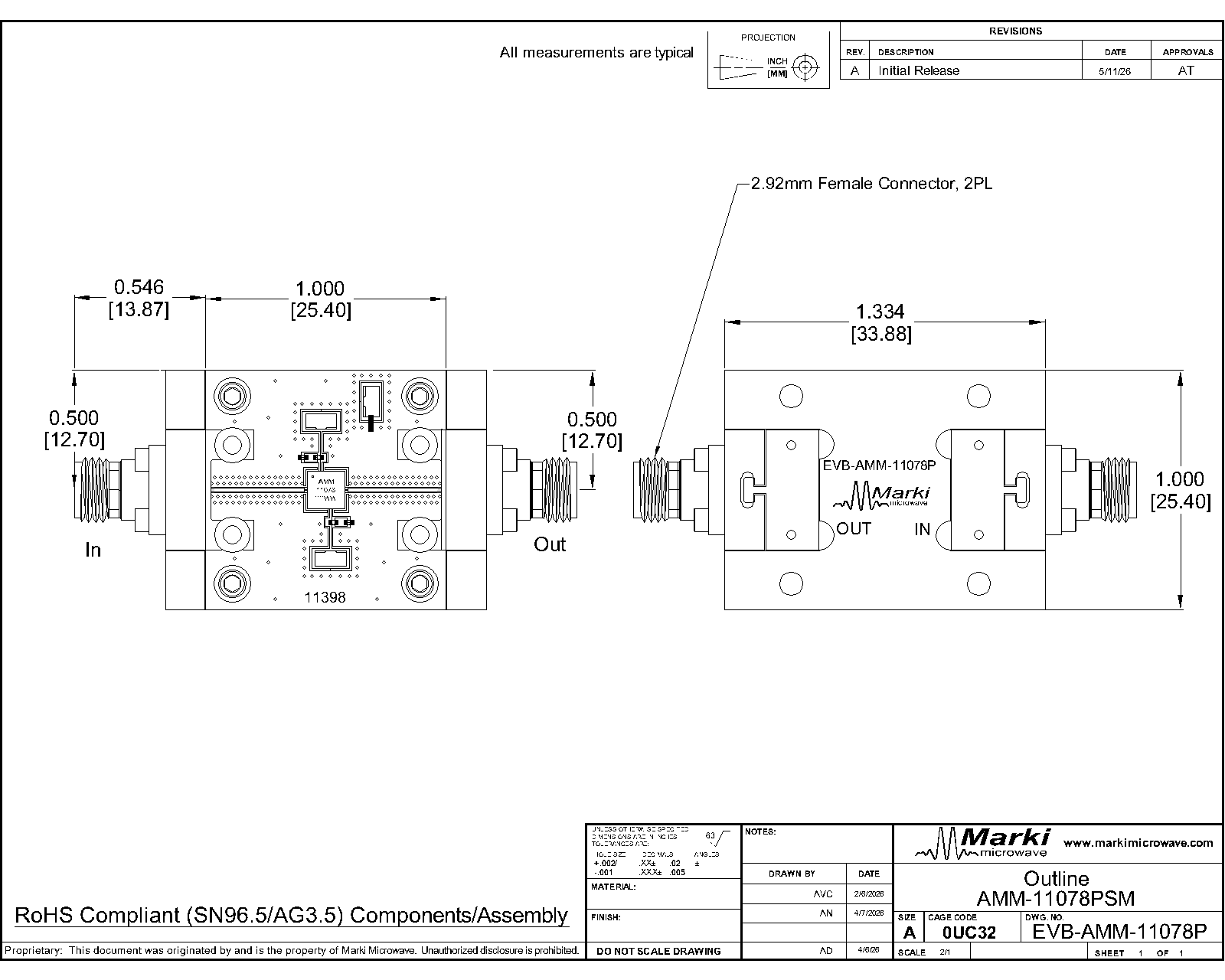
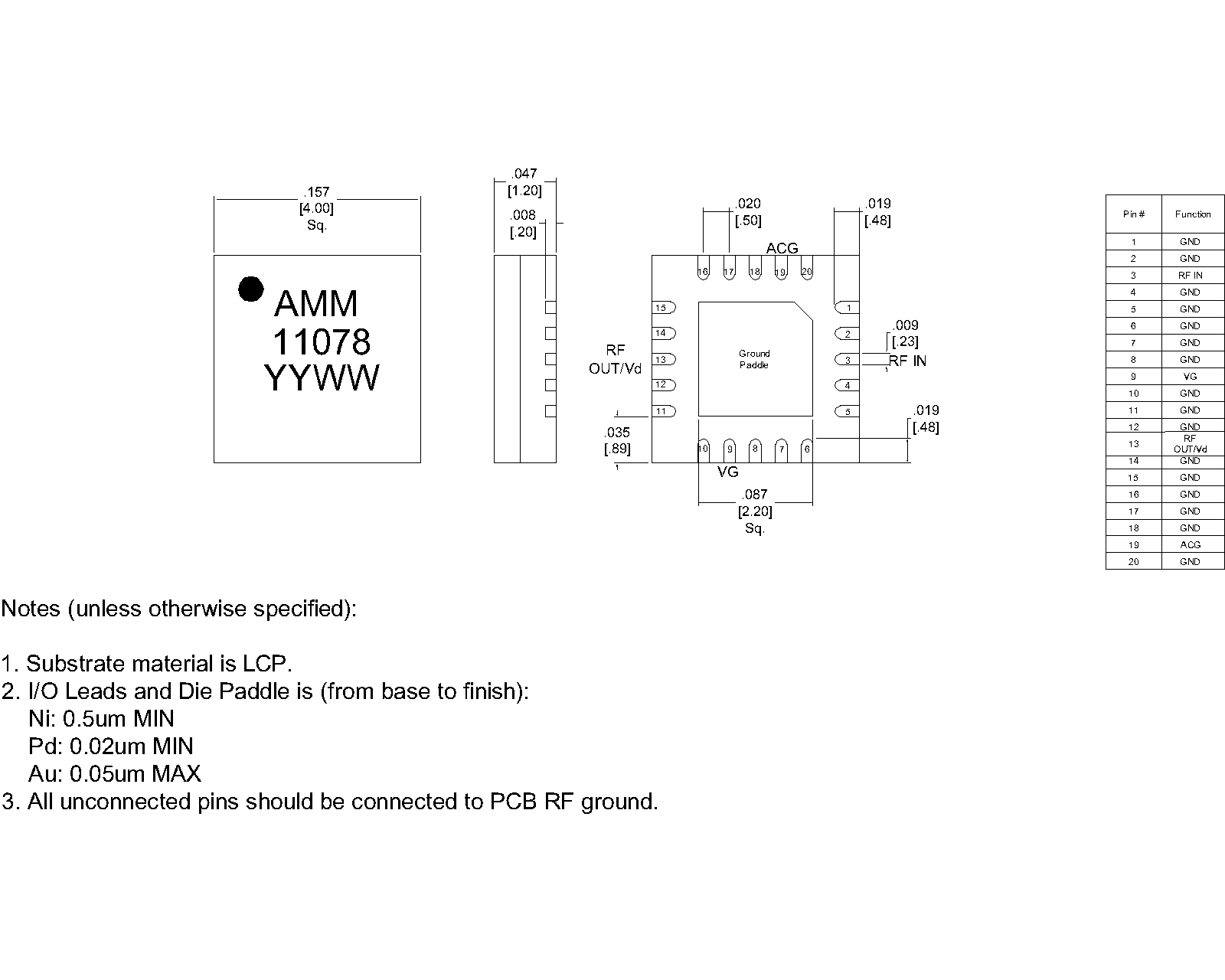
Port Diagram
A port diagram of the AMM-11078PSM QFN package is shown below (X-ray view from the top).
.png)

Sales: 408-778-9952 | General: 408-778-4200 | Fax: 408-778-4300
Sales & Customer Support: [email protected]
Tech Support: [email protected]
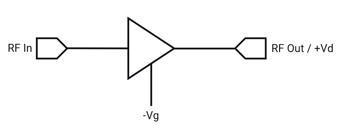
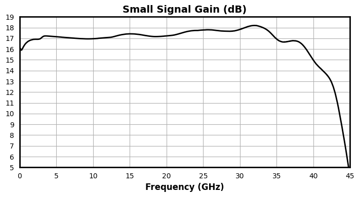
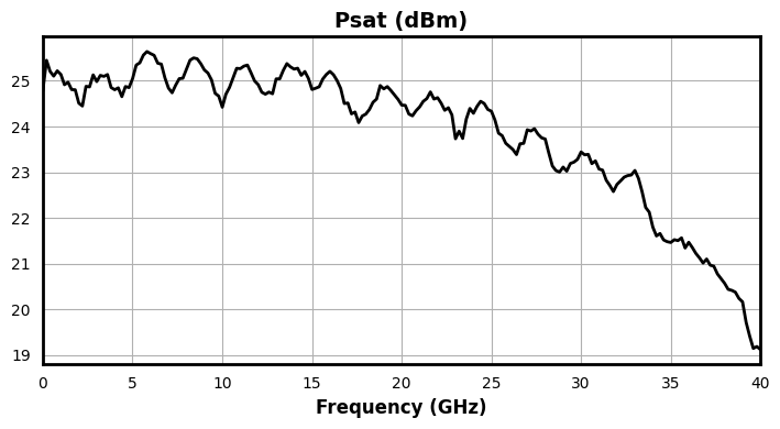
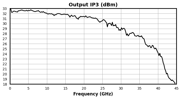
The AMM-11078PSM is a wideband GaAs distributed amplifier covering 0.01 to 40 GHz, delivering 17.2 dB small-signal gain with high output power and linearity. It provides up to +23.5 dBm saturated output power, with output IP3 up to +32.5 dBm. Operating from a +7V supply at 205 mA typical current, the amplifier is internally matched to 50 Ω at both the RF input and output ports. These features make it well-suited for wideband driver stages in RF/mmWave front ends, test and measurement instrumentation, electronic warfare, and general-purpose broadband gain block applications.

| Part Number | Description | Package | Green Status | Product Lifecycle | Export Classification |
|---|---|---|---|---|---|
| AMM-11078PSM | 0.01 - 40 GHz Surface Mount Amplifier | QFN | REACH RoHS | Released | 3A001.b.2.d |
| EVB-AMM-11078P | Evaluation Board, 0.01-40GHz Surface Mount Amplifier | EVB | REACH RoHS | Released | 3A001.b.2.d |
| Part Number | Description | Package | Green Status | Product Lifecycle | Export Classification |
|---|---|---|---|---|---|
| AMM-11078PSM | 0.01 - 40 GHz Surface Mount Amplifier | QFN | REACH RoHS | Released | 3A001.b.2.d |
| EVB-AMM-11078P | Evaluation Board, 0.01-40GHz Surface Mount Amplifier | EVB | REACH RoHS | Released | 3A001.b.2.d |
AMM-11078PSM
0.01 - 40 GHz Surface Mount Amplifier
| Revision Code | Revision Date | Comment |
|---|---|---|
| - | 2026-07-22 | Initial Release |
AMM-11078PSM
0.01 - 40 GHz Surface Mount Amplifier
A port diagram of the AMM-11078PSM QFN package is shown below (X-ray view from the top).
| Port | Function | Description | DC Equivalent Circuit |
|---|---|---|---|
| GND | Ground | QFN backside must be connected to a DC/RF ground with high thermal and electrical conductivity. |  |
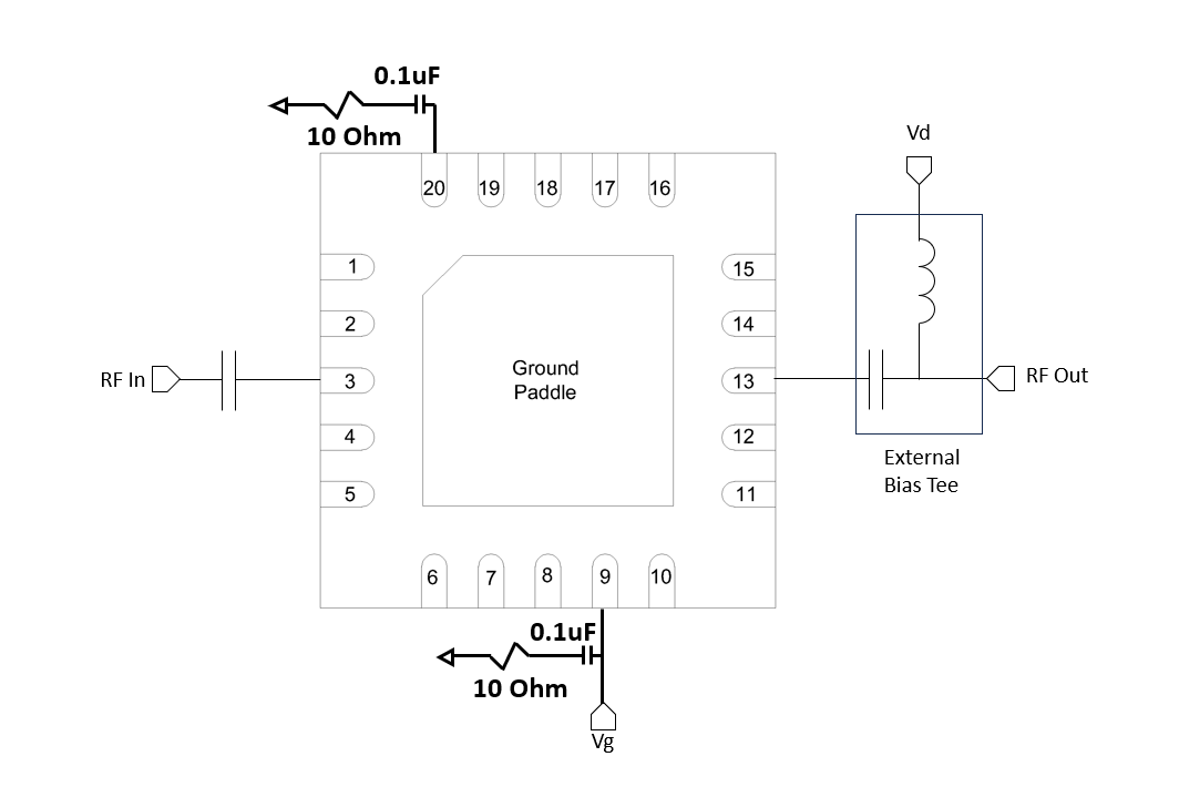
| Pin 13 | RF Out / Vd | The RF Out/ Vd pin supplies DC voltage to the drain of the amplifier and also acts as the RF output. This pin requires an external bias-tee. |  |
| Pin 19 | ACG | The ACG pin provides additional off chip bypass capacitance. A 0.1uF chip capacitor is recommended. | 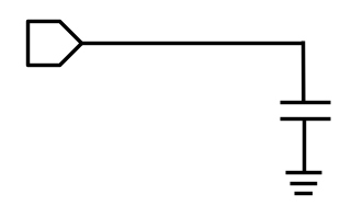 |
| Pin 3 | RF Input | This is the RF input port of the device, and is RF matched to 50 Ω and requires a DC blocking capacitor. | 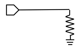 |
| Pin 9 | Vg | Gate control for the amplifier. The user should apply between -0.15V and -0.35V to Vg pin before applying positive DC voltage to any Vd port. Lower (more negative) voltages on a Vg pin will result in lower drain current and lower small signal gain. | 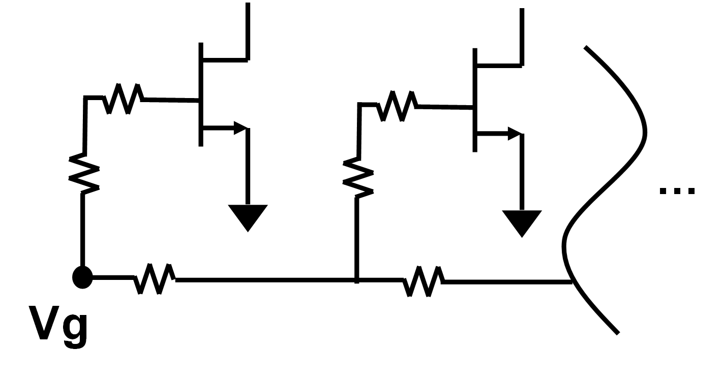 |
AMM-11078PSM
0.01 - 40 GHz Surface Mount Amplifier
The Absolute Maximum Ratings indicate limits beyond which damage may occur to the device. If any one of these limits are exceeded, the device may become inoperable or have a reduced lifetime.
| Parameter | Maximum Rating | Unit |
|---|---|---|
| Drain Current (RF Applied) | 550 | mA |
| Drain Supply Voltage (Vd) | 10 | V |
| Gate Voltage (Vg) | -0.5 | V |
| Maximum Operating Temperature for MTTF > 1E6 hours | 85 | °C |
| Maximum Storage Temperature | 150 | °C |
| Max Junction Temperature for MTTF > 1E6 Hours | 175 | °C |
| Max Power Dissipation for MTTF of 1E6 hours at 85˚C Baseplate Temperature | 3.9 | W |
| Minimum Operating Temperature for MTTF > 1E6 hours | -55 | °C |
| Minimum Storage Temperature | -65 | °C |
| RF Input Power | 18 | dBm |
| θ_Jc, Junction to Case Thermal Resistance | 23 | ºC/W |
| Parameter | Details | Rating |
|---|---|---|
| ESD | < 250 Volts | HBM Class 0 |
| Dimensions | - | 4 x 4 mm |
| Moisture Sensitivity Level | - | MSL 1 |
The Recommended Operating Conditions indicate the limits, inside which the device should be operated, to guarantee the performance given in Electrical Specifications Operating outside these limits may not necessarily cause damage to the device, but the performance may degrade outside the limits of the electrical specifications. For limits, above which damage may occur, see Absolute Maximum Ratings. Power Supply DC current should be modified by changing bias voltage Vg to maintain junction temperature within MTTF target for given operating conditions.
| Parameter | Min | Nominal | Max | Unit |
|---|---|---|---|---|
| Ambient Temperature | -40 | 25 | 85 | °C |
| Power Supply DC Voltage | 4 | 7 | 8 | V |
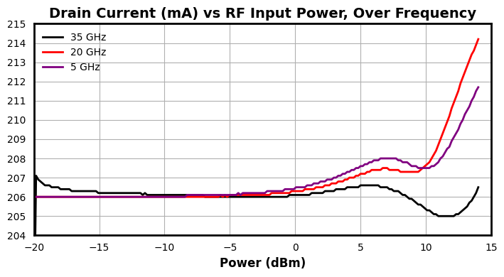
| Power Supply DC Current (Id) (No RF Input) | 150 | 205 | 220 | mA |
| Negative Bias Voltage (Vg) | -0.35 | -0.25 | -0.15 | V |
| Input Power for Saturation | 10 | 11 | 15 | dBm |
AMM-11078PSM
0.01 - 40 GHz Surface Mount Amplifier
Unless otherwise specified, electrical specifications apply at TA=+25°C, Vd = 7 V, Vg set as required to achieve Id = 205 mA in a 50 Ω system.
| Parameter | Test Conditions | Minimum Frequency (GHz) | Maximum Frequency (GHz) | Min | Typ | Max | Unit |
|---|---|---|---|---|---|---|---|
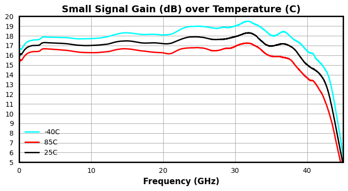
| Small Signal Gain | Pin = -15 dBm | 0.01 | 40 | - | 17.2 | - | dB |
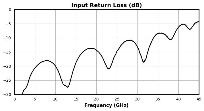
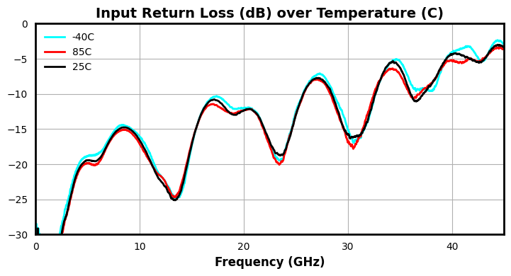
| Input Return Loss | Pin = -15 dBm | 0.01 | 40 | - | 17 | - | dB |
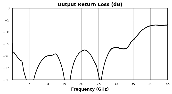
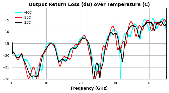
| Output Return Loss | Pin = -15 dBm | 0.01 | 40 | - | 20 | - | dB |
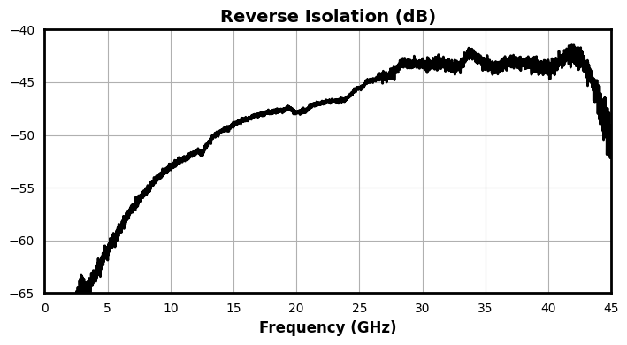
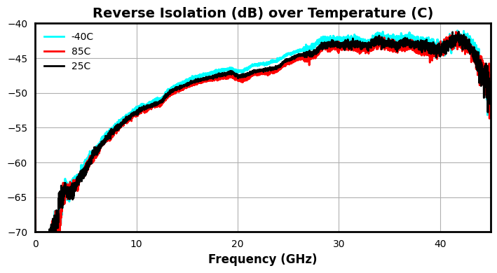
| Reverse Isolation | Pin = -15 dBm | 0.01 | 40 | - | 20 | - | dB |
| Saturated Output Power | Pin = 11 dBm | 0.01 | 40 | - | 23.46 | - | dBm |
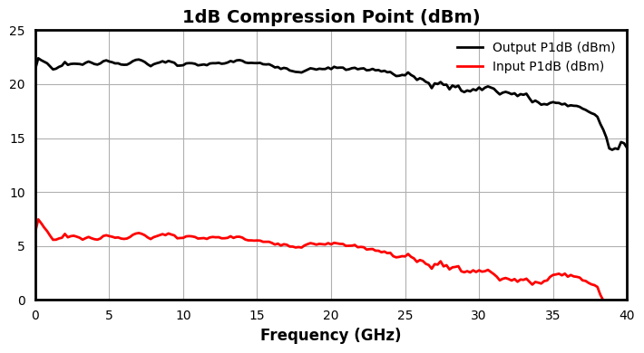
| Input P1dB | - | 0.01 | 40 | - | 5 | - | dBm |
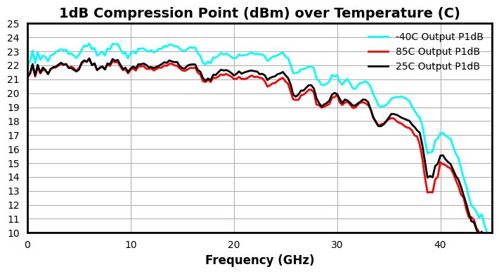
| Output P1dB | - | 0.01 | 40 | - | 21.5 | - | dBm |
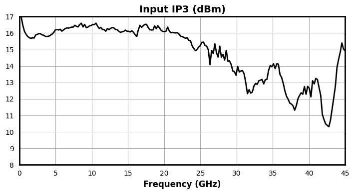
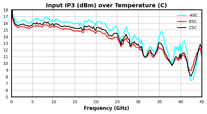
| Input IP3 | Pin -8 dBm, 1 MHz Tone Spacing | 0.01 | 40 | - | 15 | - | dBm |
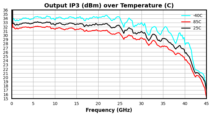
| Output IP3 | Pin -8 dBm, 1 MHz Tone Spacing | 0.01 | 40 | - | 32.5 | - | dBm |
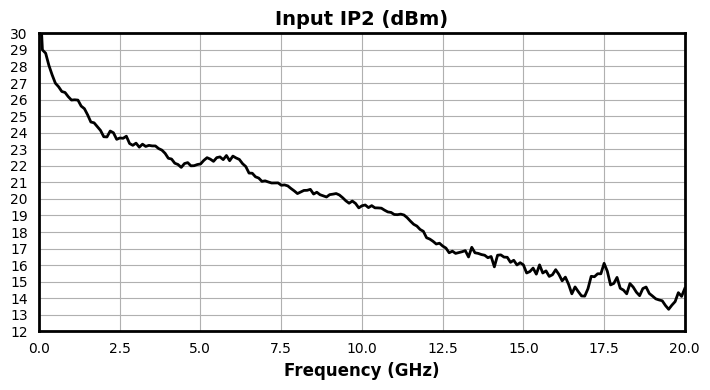
| Input IP2 | Pin -8 dBm, 1 MHz Tone Spacing | 0.01 | 40 | - | 19.5 | - | dBm |
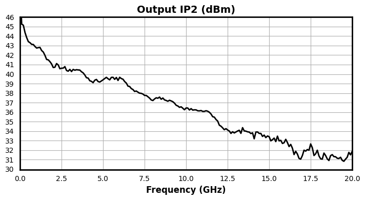
| Output IP2 | Pin -8 dBm, 1 MHz Tone Spacing | 0.01 | 40 | - | 36.5 | - | dBm |
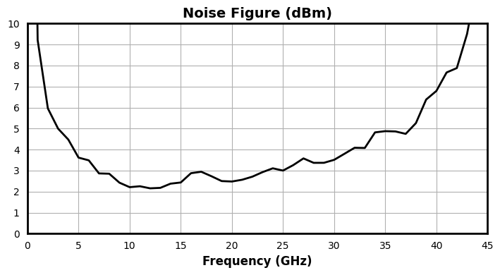
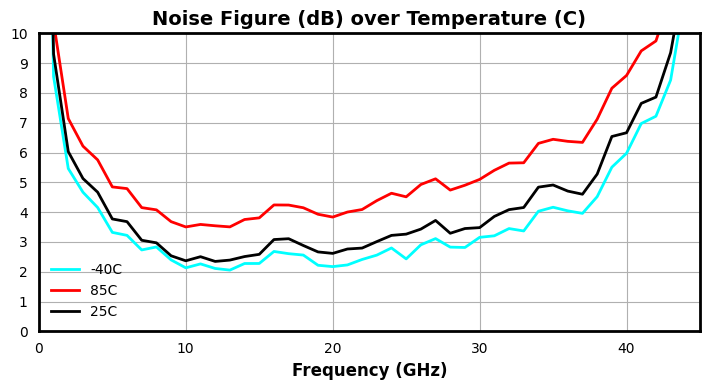
| Noise Figure | Pin = -15 dBm | 0.01 | 40 | - | 3.3 | - | dB |
| Current Consumption | - | 0.01 | 40 | - | 205 | - | mA |
| Parameter | Test Conditions | Minimum Frequency (GHz) | Maximum Frequency (GHz) | Min | Typ | Max | Unit |
|---|---|---|---|---|---|---|---|
| Small Signal Gain | Pin = -15 dBm | 0.01 | 40 | - | 17.2 | - | dB |
| Input Return Loss | Pin = -15 dBm | 0.01 | 40 | - | 17 | - | dB |
| Output Return Loss | Pin = -15 dBm | 0.01 | 40 | - | 20 | - | dB |
| Reverse Isolation | Pin = -15 dBm | 0.01 | 40 | - | 20 | - | dB |
| Saturated Output Power | Pin = 11 dBm | 0.01 | 40 | - | 23.46 | - | dBm |
| Input P1dB | - | 0.01 | 40 | - | 5 | - | dBm |
| Output P1dB | - | 0.01 | 40 | - | 21.5 | - | dBm |
| Input IP3 | Pin -8 dBm, 1 MHz Tone Spacing | 0.01 | 40 | - | 15 | - | dBm |
| Output IP3 | Pin -8 dBm, 1 MHz Tone Spacing | 0.01 | 40 | - | 32.5 | - | dBm |
| Input IP2 | Pin -8 dBm, 1 MHz Tone Spacing | 0.01 | 40 | - | 19.5 | - | dBm |
| Output IP2 | Pin -8 dBm, 1 MHz Tone Spacing | 0.01 | 40 | - | 36.5 | - | dBm |
| Noise Figure | Pin = -15 dBm | 0.01 | 40 | - | 3.3 | - | dB |
| Current Consumption | - | 0.01 | 40 | - | 205 | - | mA |
AMM-11078PSM
0.01 - 40 GHz Surface Mount Amplifier
AMM-11078PSM
0.01 - 40 GHz Surface Mount Amplifier
AMM-11078PSM
0.01 - 40 GHz Surface Mount Amplifier
AMM-11078PSM
0.01 - 40 GHz Surface Mount Amplifier
AMM-11078PSM
0.01 - 40 GHz Surface Mount Amplifier
AMM-11078PSM
0.01 - 40 GHz Surface Mount Amplifier
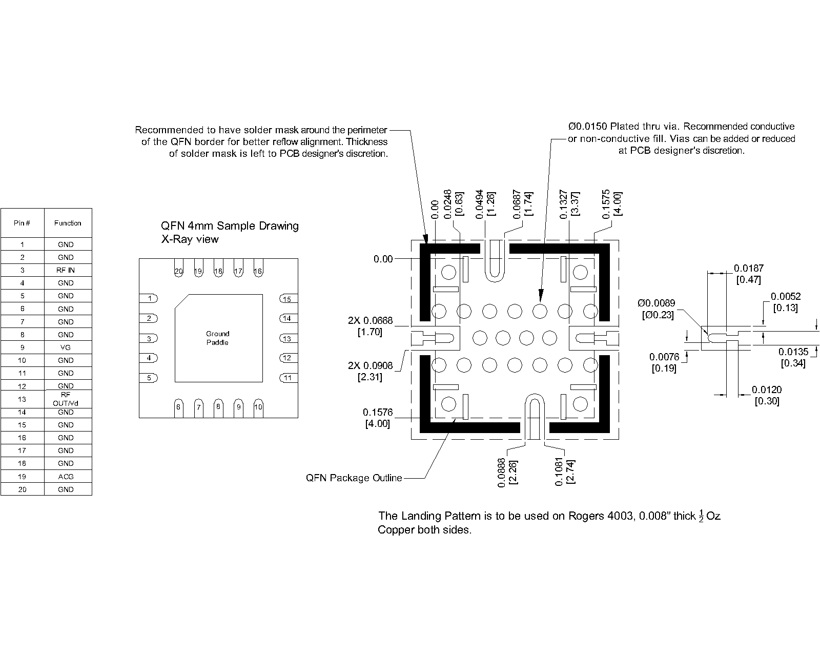
Download : Footprint Drawing
AMM-11078PSM
0.01 - 40 GHz Surface Mount Amplifier