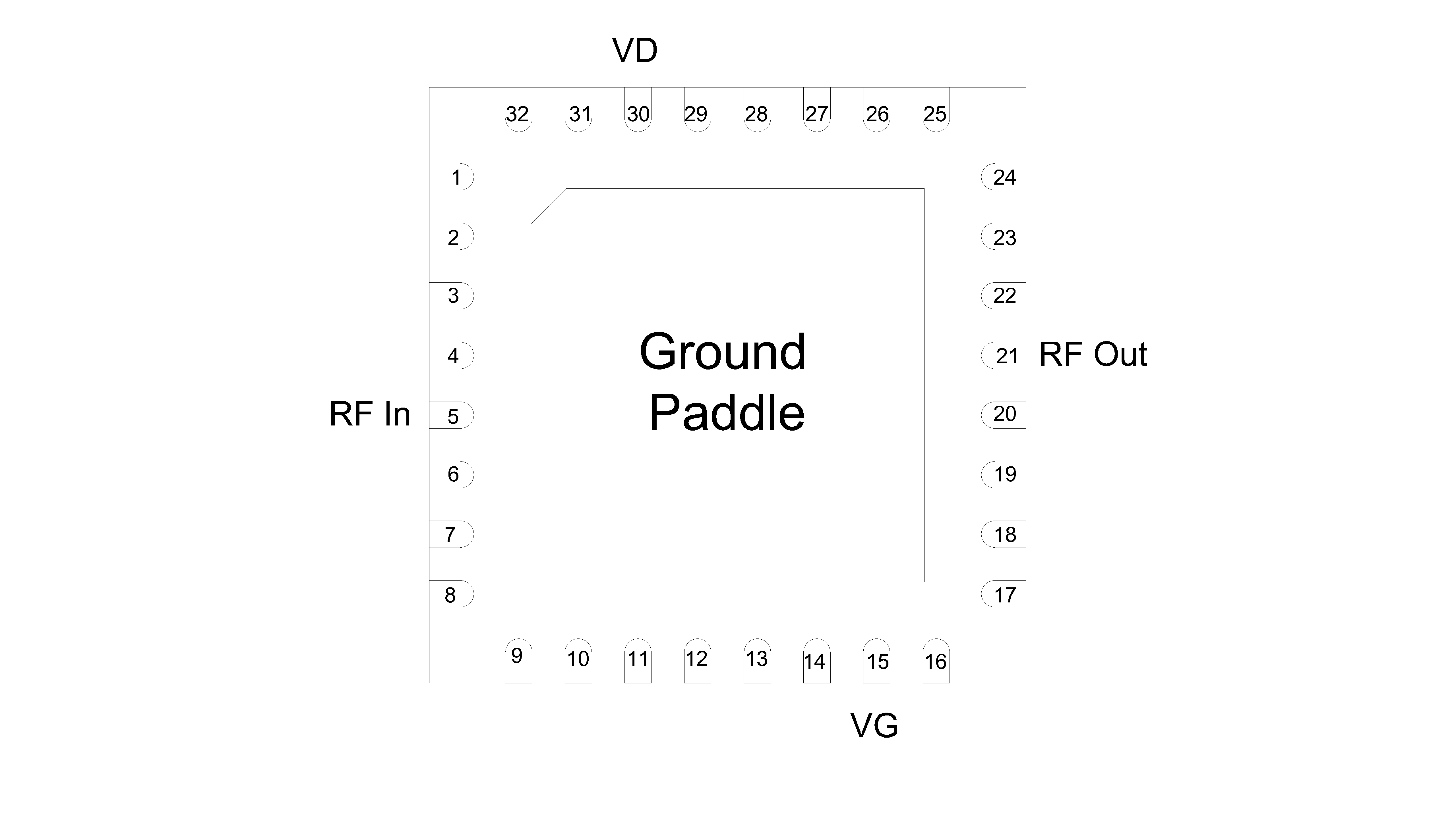
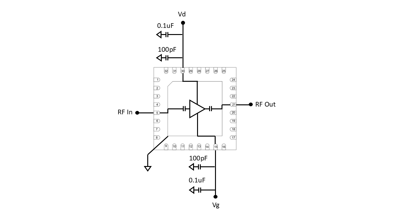
Port Diagram
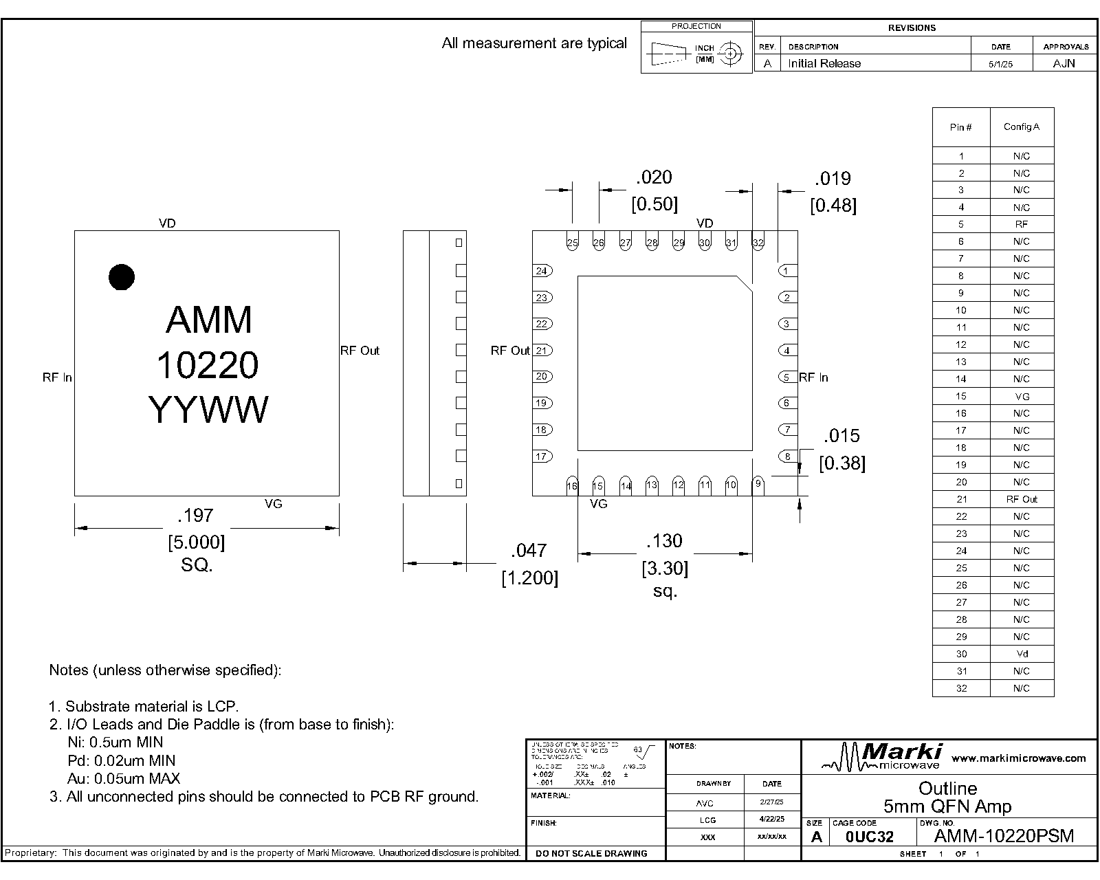
A port diagram of the AMM-10220PSM QFN package is shown below (X-ray view from the top).
Sales: 408-778-9952 | General: 408-778-4200 | Fax: 408-778-4300
Sales & Customer Support: [email protected]
Tech Support: [email protected]
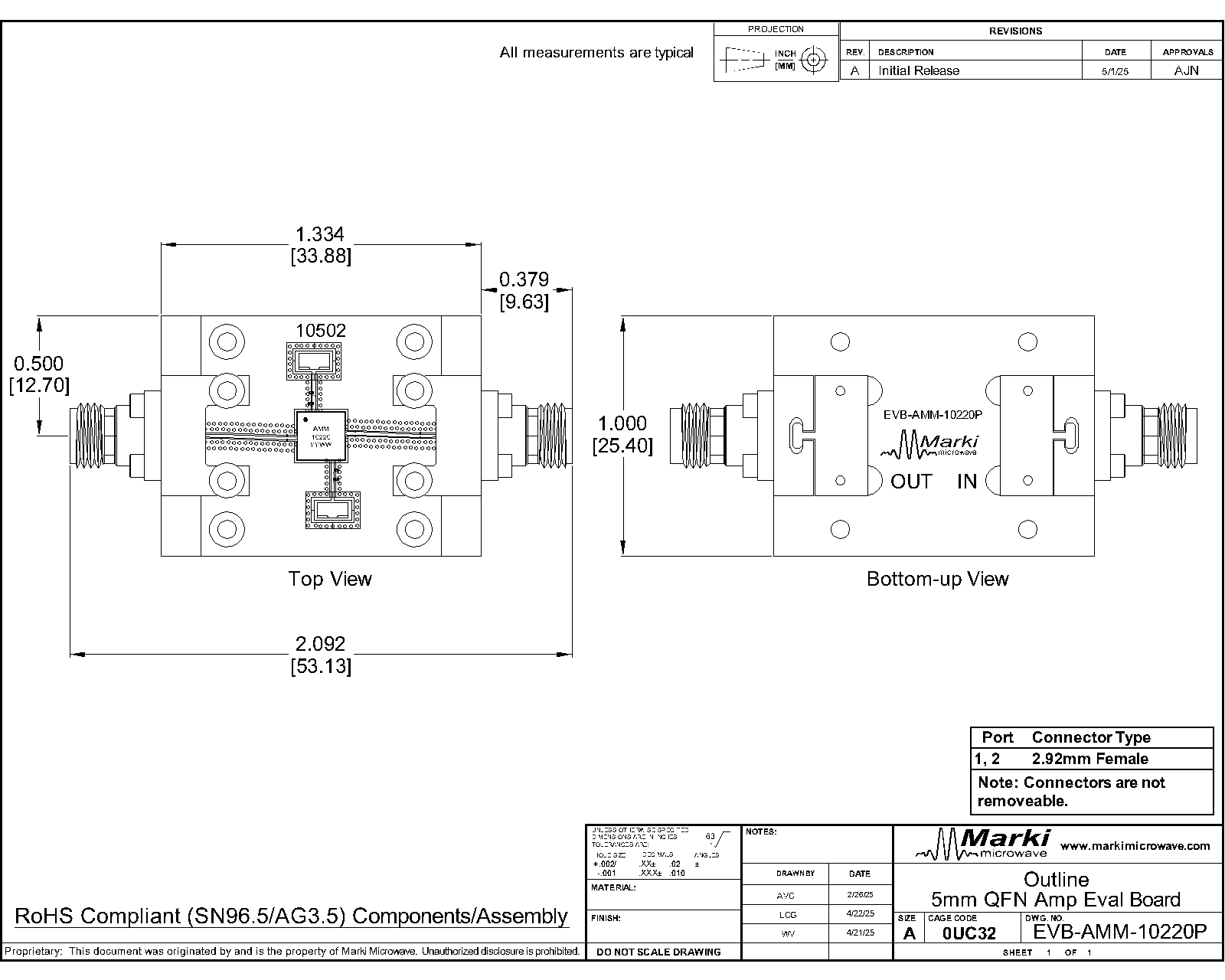
The AMM-10220PSM is a surface-mount amplifier suitable for use as a single tone driver or general-purpose gain block. It can drive an L or H diode mixer from 2 to 26 GHz. This amplifier also has exceptionally low input and output reflections, and a low 2.7 dB typical noise figure from 8 to 18 GHz. Additionally, this amplifier exhibits a positive gain slope to equalize frequency dependent losses. The AMM-10220PSM is packaged in a compact 5 mm QFN for surface mount integration onto printed circuit boards.


| Part Number | Description | Package | Green Status | Product Lifecycle | Export Classification |
|---|---|---|---|---|---|
| AMM-10220PSM | 2 - 26 GHz GaAs Surface Mount LO Driver Amplifier | QFN | REACH RoHS | Released | EAR99 |
| EVB-AMM-10220P | Evaluation Board, AMM-10220PSM, 2 - 26 GHz GaAs Surface Mount LO Driver Amplifier | - | REACH RoHS | Released | - |
AMM-10220PSM
2 - 26 GHz GaAs Surface Mount LO Driver Amplifier
| Revision Code | Revision Date | Comment |
|---|---|---|
| - | 2025-09-02 | Initial Release |
AMM-10220PSM
2 - 26 GHz GaAs Surface Mount LO Driver Amplifier
A port diagram of the AMM-10220PSM QFN package is shown below (X-ray view from the top).
| Port | Function | Description | DC Equivalent Circuit |
|---|---|---|---|
| Pin 1-4, 6-14, 16-20, 22-29, 31, 32, Paddle | Ground | These pins should be connected to ground. Package ground paddle must be connected to a DC/RF ground potential with high thermal and electrical conductivity. | - |
| Pin 15 | Vg | Pin 15 provides a required negative bias which controls the power supply currents to the amplifier. More negative voltages decrease supply current. Apply gate bias voltage Vg before applying drain power supply. |  |
| Pin 21 | RF Output | Pin 21 is the RF Output port of the amplifier. It is DC blocked, and RF matched to 50 Ω. |  |
| Pin 30 | Vd | Pin 30 provides the main power supply for the amplifier. Apply gate bias voltage Vg before applying drain power supply. |  |
| Pin 5 | RF Input | Pin 5 is the RF Input port of the amplifier die. It is internally DC blocked and RF matched to 50 Ω. | |
AMM-10220PSM
2 - 26 GHz GaAs Surface Mount LO Driver Amplifier
The Absolute Maximum Ratings indicate limits beyond which damage may occur to the device. If any one of these limits are exceeded, the device may become inoperable or have a reduced lifetime.
| Parameter | Maximum Rating | Unit |
|---|---|---|
| Drain Current (RF Applied) | 130 | mA |
| Drain Supply Voltage (Vd) | 6 | V |
| Gate Voltage (Vg) | -1 | V |
| Maximum Operating Temperature for MTTF > 1E6 hours | 85 | °C |
| Maximum Storage Temperature | 150 | °C |
| Minimum Operating Temperature for MTTF > 1E6 hours | -55 | °C |
| Minimum Storage Temperature | -65 | °C |
| RF Input Power | 20 | dBm |
| Parameter | Details | Rating |
|---|---|---|
| Dimensions | - | 5 x 5 mm |
| Moisture Sensitivity Level | - | MSL 1 |
Datasheet operating parameters are taken and guaranteed using constant voltage biasing with TA = 25 °C, Vd = 5 V, Idq = 74 mA, and 50 Ω matched input and output. Adjust Vg from −1 V to -0.3 V max to achieve Idq = 74 mA typical.
| Parameter | Min | Nominal | Max | Unit |
|---|---|---|---|---|
| Negative Bias Voltage (Vg) | -0.5 | -0.4 | -0.3 | V |
| Positive DC Current (Id) (No RF Input) | - | 74 | - | mA |
| Positive DC Voltage (Vd) | - | 5 | - | V |
| Operating Temperature | -40 | 25 | 85 | °C |
AMM-10220PSM
2 - 26 GHz GaAs Surface Mount LO Driver Amplifier
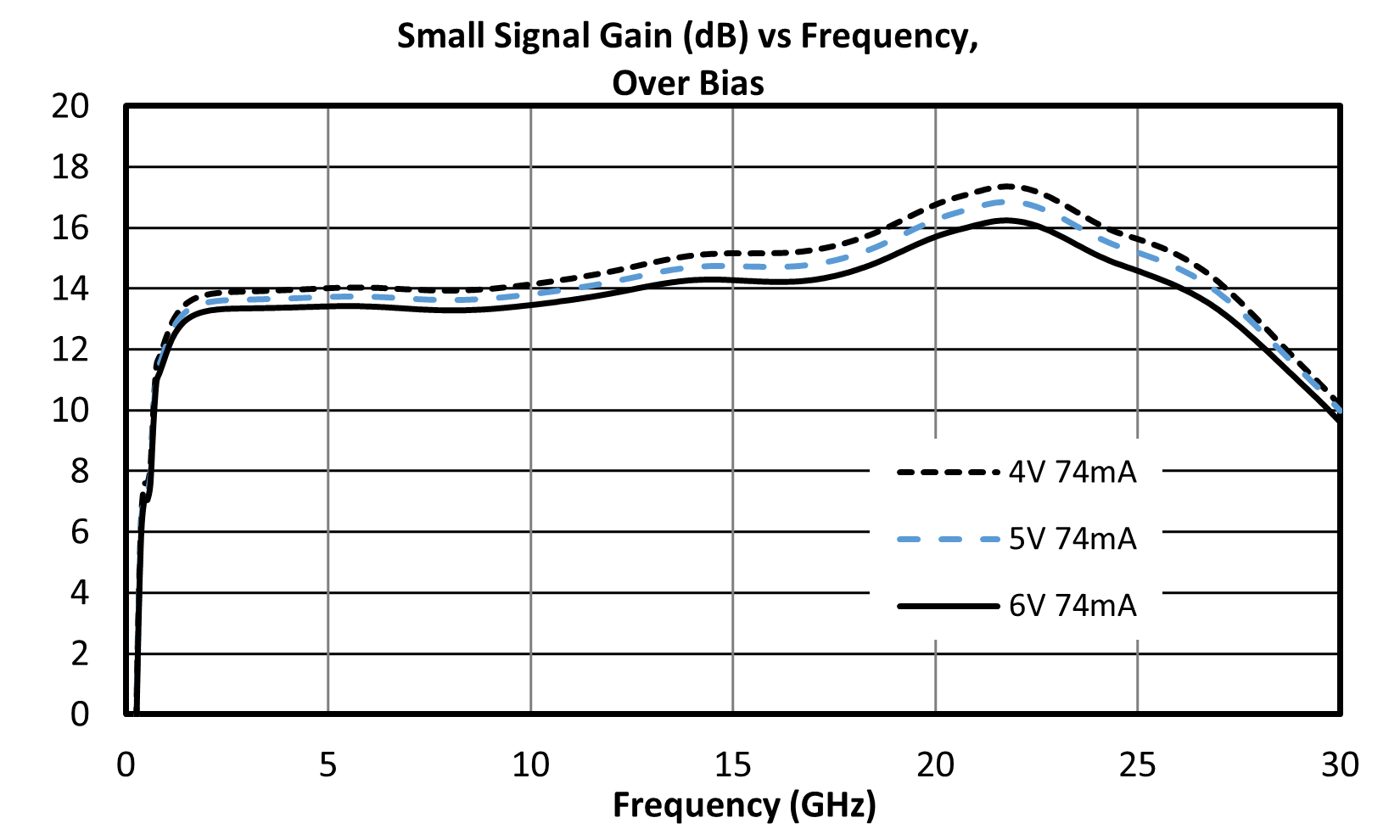
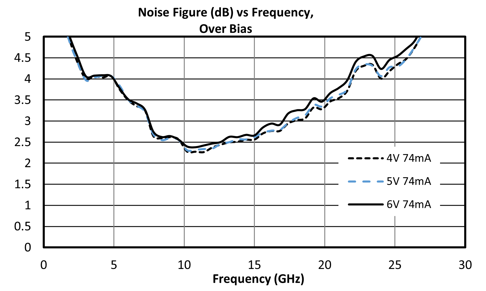
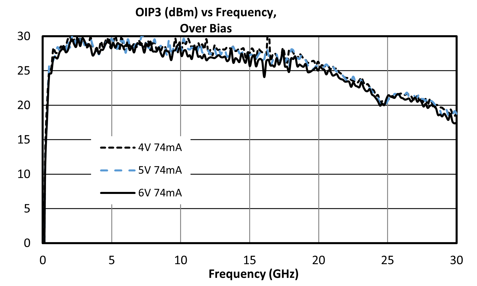
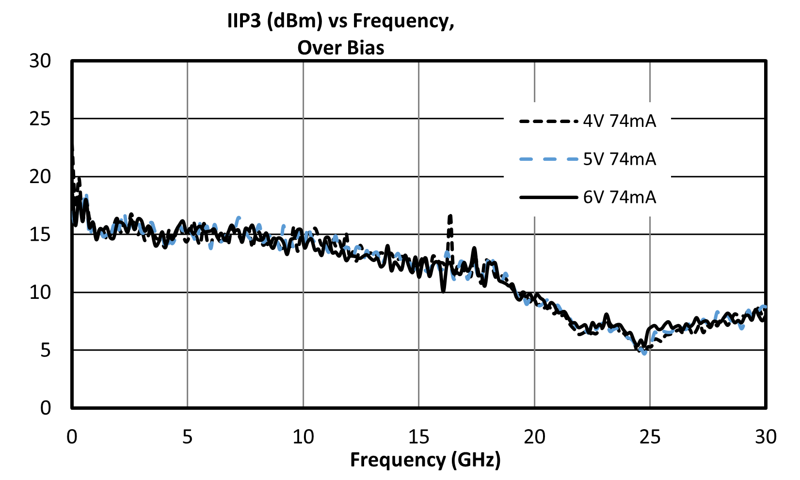
Unless otherwise specified, electrical specifications apply at TA=+25°C, Vd = 5 V, Idq=74 mA (where Idq is the drain current with no RF applied), Vg set as required to achieve Idq = 74 mA in a 50 Ω system.
| Parameter | Test Conditions | Minimum Frequency (GHz) | Maximum Frequency (GHz) | Min | Typ | Max | Unit |
|---|---|---|---|---|---|---|---|
| Current Consumption | Vd = 5 V, Vg = -0.4V, No RF Applied | - | - | - | 74 | - | mA |
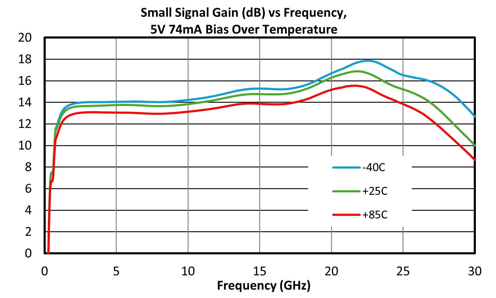
| Small Signal Gain | Vd = 5 V, Vg set to achieve Idq = 74 mA, Pin = -20 dBm | 2 | 8 | - | 14 | - | dB |
| Small Signal Gain | Vd = 5 V, Vg set to achieve Idq = 74 mA, Pin = -20 dBm | 8 | 18 | - | 14.5 | - | dB |
| Small Signal Gain | Vd = 5 V, Vg set to achieve Idq = 74 mA, Pin = -20 dBm | 18 | 26 | - | 16 | - | dB |
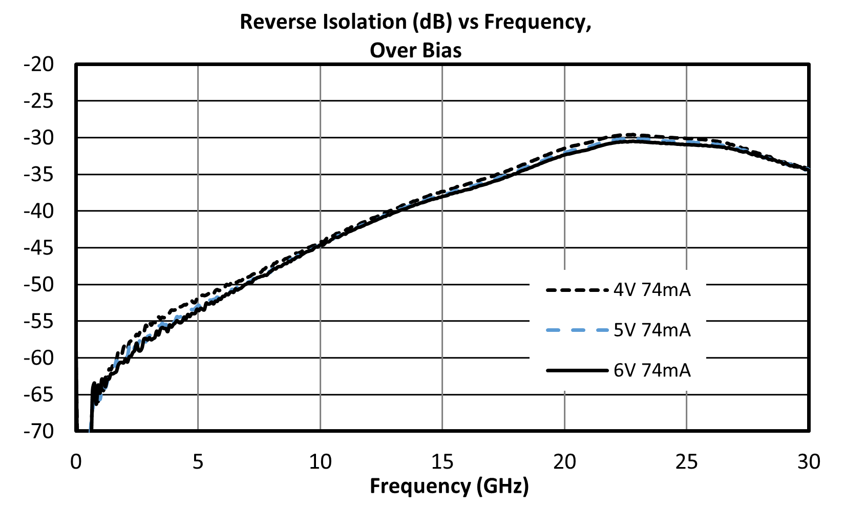
| Reverse Isolation | Vd = 5 V, Vg set to achieve Idq = 74 mA, Pin = -20 dBm | 2 | 8 | - | 53 | - | dB |
| Reverse Isolation | Vd = 5 V, Vg set to achieve Idq = 74 mA, Pin = -20 dBm | 8 | 18 | - | 43 | - | dB |
| Reverse Isolation | Vd = 5 V, Vg set to achieve Idq = 74 mA, Pin = -20 dBm | 18 | 26 | - | 33 | - | dB |
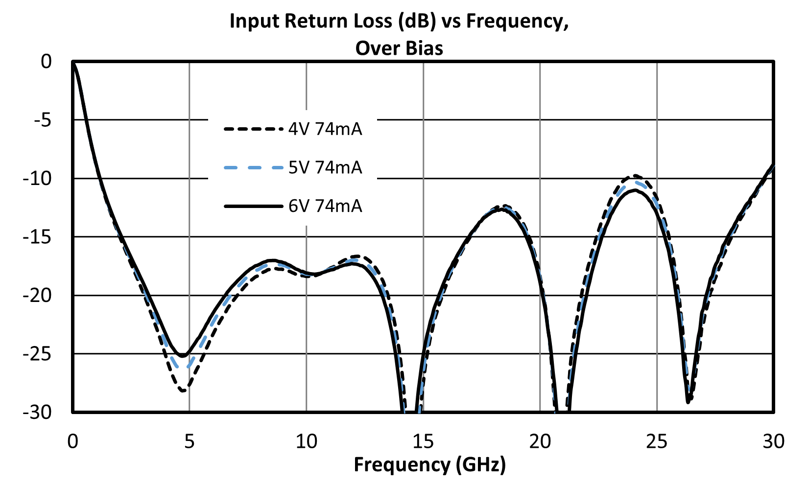
| Input Return Loss | Vd = 5 V, Vg set to achieve Idq = 74 mA, Pin = -20 dBm | 2 | 8 | - | 17 | - | dB |
| Input Return Loss | Vd = 5 V, Vg set to achieve Idq = 74 mA, Pin = -20 dBm | 8 | 18 | - | 16 | - | dB |
| Input Return Loss | Vd = 5 V, Vg set to achieve Idq = 74 mA, Pin = -20 dBm | 18 | 26 | - | 14 | - | dB |
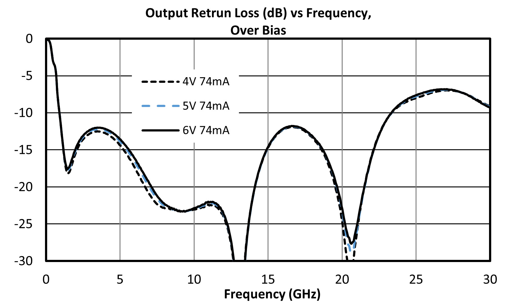
| Output Return Loss | Vd = 5 V, Vg set to achieve Idq = 74 mA, Pin = -20 dBm | 2 | 8 | - | 18 | - | dB |
| Output Return Loss | Vd = 5 V, Vg set to achieve Idq = 74 mA, Pin = -20 dBm | 8 | 18 | - | 18 | - | dB |
| Output Return Loss | Vd = 5 V, Vg set to achieve Idq = 74 mA, Pin = -20 dBm | 18 | 26 | - | 14 | - | dB |
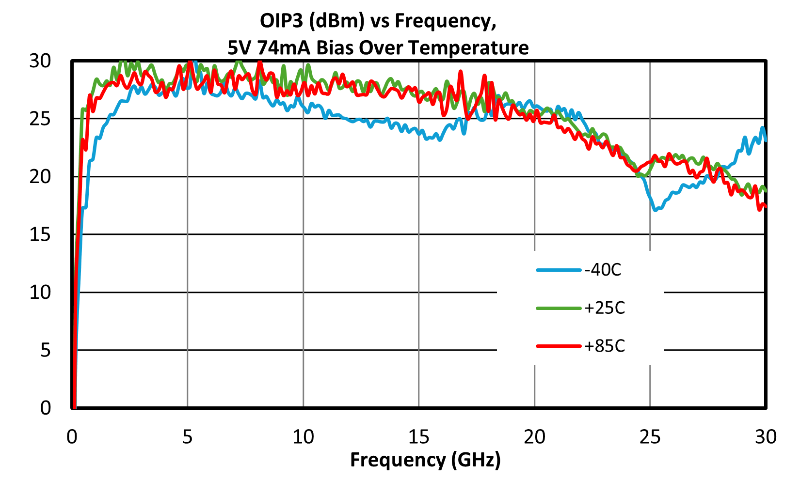
| Output IP3 | Vd = 5 V, Vg set to achieve Idq = 74 mA, Pin = -15 dBm per tone, 10 MHz tone spacing | 2 | 8 | - | 28 | - | dBm |
| Output IP3 | Vd = 5 V, Vg set to achieve Idq = 74 mA, Pin = -15 dBm per tone, 10 MHz tone spacing | 8 | 18 | - | 28 | - | dBm |
| Output IP3 | Vd = 5 V, Vg set to achieve Idq = 74 mA, Pin = -15 dBm per tone, 10 MHz tone spacing | 18 | 26 | - | 24 | - | dBm |
| Input IP3 | Vd = 5 V, Vg set to achieve Idq = 74 mA, Pin = -15 dBm per tone, 10 MHz tone spacing | 2 | 8 | - | 15 | - | dBm |
| Input IP3 | Vd = 5 V, Vg set to achieve Idq = 74 mA, Pin = -15 dBm per tone, 10 MHz tone spacing | 8 | 18 | - | 13.5 | - | dBm |
| Input IP3 | Vd = 5 V, Vg set to achieve Idq = 74 mA, Pin = -15 dBm per tone, 10 MHz tone spacing | 18 | 26 | - | 7.5 | - | dBm |
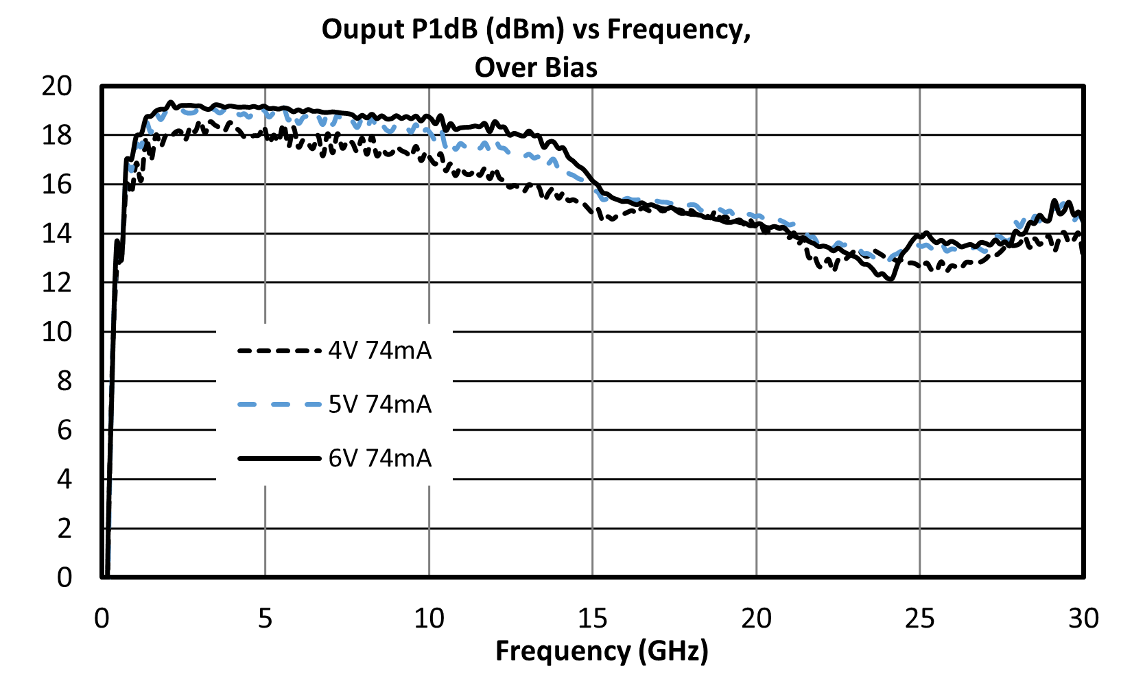
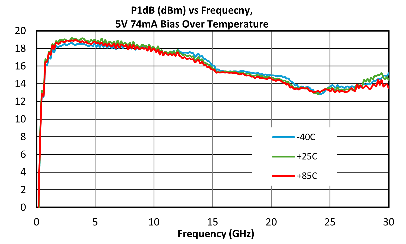
| Output P1dB | Vd = 5 V, Vg set to achieve Idq = 74 mA | 2 | 14 | - | 18 | - | dBm |
| Output P1dB | Vd = 5 V, Vg set to achieve Idq = 74 mA | 14 | 26 | - | 15.5 | - | dBm |
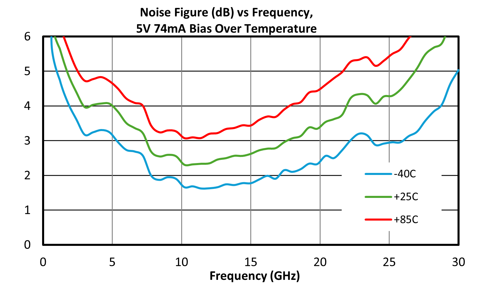
| Noise Figure | Vd = 5 V, Vg set to achieve Idq = 74 mA, Pin = -20 dBm | 2 | 8 | - | 3.4 | - | dB |
| Noise Figure | Vd = 5 V, Vg set to achieve Idq = 74 mA, Pin = -20 dBm | 8 | 18 | - | 2.7 | - | dB |
| Noise Figure | Vd = 5 V, Vg set to achieve Idq = 74 mA, Pin = -20 dBm | 18 | 26 | - | 3.6 | - | dB |
| Parameter | Test Conditions | Minimum Frequency (GHz) | Maximum Frequency (GHz) | Min | Typ | Max | Unit |
|---|---|---|---|---|---|---|---|
| Current Consumption | Vd = 5 V, Vg = -0.4V, No RF Applied | - | - | - | 74 | - | mA |
| Small Signal Gain | Vd = 5 V, Vg set to achieve Idq = 74 mA, Pin = -20 dBm | 2 | 8 | - | 14 | - | dB |
| Small Signal Gain | Vd = 5 V, Vg set to achieve Idq = 74 mA, Pin = -20 dBm | 8 | 18 | - | 14.5 | - | dB |
| Small Signal Gain | Vd = 5 V, Vg set to achieve Idq = 74 mA, Pin = -20 dBm | 18 | 26 | - | 16 | - | dB |
| Reverse Isolation | Vd = 5 V, Vg set to achieve Idq = 74 mA, Pin = -20 dBm | 2 | 8 | - | 53 | - | dB |
| Reverse Isolation | Vd = 5 V, Vg set to achieve Idq = 74 mA, Pin = -20 dBm | 8 | 18 | - | 43 | - | dB |
| Reverse Isolation | Vd = 5 V, Vg set to achieve Idq = 74 mA, Pin = -20 dBm | 18 | 26 | - | 33 | - | dB |
| Input Return Loss | Vd = 5 V, Vg set to achieve Idq = 74 mA, Pin = -20 dBm | 2 | 8 | - | 17 | - | dB |
| Input Return Loss | Vd = 5 V, Vg set to achieve Idq = 74 mA, Pin = -20 dBm | 8 | 18 | - | 16 | - | dB |
| Input Return Loss | Vd = 5 V, Vg set to achieve Idq = 74 mA, Pin = -20 dBm | 18 | 26 | - | 14 | - | dB |
| Output Return Loss | Vd = 5 V, Vg set to achieve Idq = 74 mA, Pin = -20 dBm | 2 | 8 | - | 18 | - | dB |
| Output Return Loss | Vd = 5 V, Vg set to achieve Idq = 74 mA, Pin = -20 dBm | 8 | 18 | - | 18 | - | dB |
| Output Return Loss | Vd = 5 V, Vg set to achieve Idq = 74 mA, Pin = -20 dBm | 18 | 26 | - | 14 | - | dB |
| Output IP3 | Vd = 5 V, Vg set to achieve Idq = 74 mA, Pin = -15 dBm per tone, 10 MHz tone spacing | 2 | 8 | - | 28 | - | dBm |
| Output IP3 | Vd = 5 V, Vg set to achieve Idq = 74 mA, Pin = -15 dBm per tone, 10 MHz tone spacing | 8 | 18 | - | 28 | - | dBm |
| Output IP3 | Vd = 5 V, Vg set to achieve Idq = 74 mA, Pin = -15 dBm per tone, 10 MHz tone spacing | 18 | 26 | - | 24 | - | dBm |
| Input IP3 | Vd = 5 V, Vg set to achieve Idq = 74 mA, Pin = -15 dBm per tone, 10 MHz tone spacing | 2 | 8 | - | 15 | - | dBm |
| Input IP3 | Vd = 5 V, Vg set to achieve Idq = 74 mA, Pin = -15 dBm per tone, 10 MHz tone spacing | 8 | 18 | - | 13.5 | - | dBm |
| Input IP3 | Vd = 5 V, Vg set to achieve Idq = 74 mA, Pin = -15 dBm per tone, 10 MHz tone spacing | 18 | 26 | - | 7.5 | - | dBm |
| Output P1dB | Vd = 5 V, Vg set to achieve Idq = 74 mA | 2 | 14 | - | 18 | - | dBm |
AMM-10220PSM
2 - 26 GHz GaAs Surface Mount LO Driver Amplifier
| Parameter | Test Conditions | Minimum Frequency (GHz) | Maximum Frequency (GHz) | Min | Typ | Max | Unit |
|---|---|---|---|---|---|---|---|
| Output P1dB | Vd = 5 V, Vg set to achieve Idq = 74 mA | 14 | 26 | - | 15.5 | - | dBm |
| Noise Figure | Vd = 5 V, Vg set to achieve Idq = 74 mA, Pin = -20 dBm | 2 | 8 | - | 3.4 | - | dB |
| Noise Figure | Vd = 5 V, Vg set to achieve Idq = 74 mA, Pin = -20 dBm | 8 | 18 | - | 2.7 | - | dB |
| Noise Figure | Vd = 5 V, Vg set to achieve Idq = 74 mA, Pin = -20 dBm | 18 | 26 | - | 3.6 | - | dB |
AMM-10220PSM
2 - 26 GHz GaAs Surface Mount LO Driver Amplifier
Performance plots have PCB trace losses de-embedded.
AMM-10220PSM
2 - 26 GHz GaAs Surface Mount LO Driver Amplifier
AMM-10220PSM
2 - 26 GHz GaAs Surface Mount LO Driver Amplifier
AMM-10220PSM
2 - 26 GHz GaAs Surface Mount LO Driver Amplifier
AMM-10220PSM
2 - 26 GHz GaAs Surface Mount LO Driver Amplifier
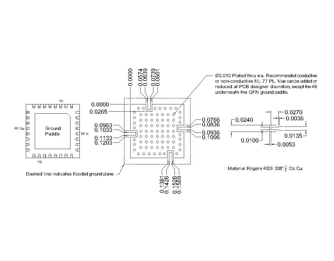
Download : Footprint Drawing
AMM-10220PSM
2 - 26 GHz GaAs Surface Mount LO Driver Amplifier