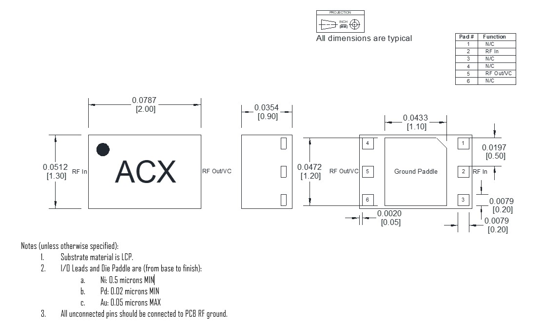
Port Diagram
A port diagram of the AKA-1500PSM is shown below.

Sales: 408-778-9952 | General: 408-778-4200 | Fax: 408-778-4300
Sales & Customer Support: [email protected]
Tech Support: [email protected]
The AKA-1500PSM is a low-cost, cascadable broadband InGaP HBT amplifier. This is a general-purpose gain block amplifier which provides high P1dB, high OIP3, and a very small form factor. The simple application circuit requires minimal external components, allowing it to be used in a variety of applications.


| Part Number | Description | Package | Green Status | Product Lifecycle | Export Classification |
|---|---|---|---|---|---|
| AKA-1500PSM | DC – 14 GHz Broadband InGaP SMT Amplifier | DFN | REACH RoHS | Released | EAR99 |
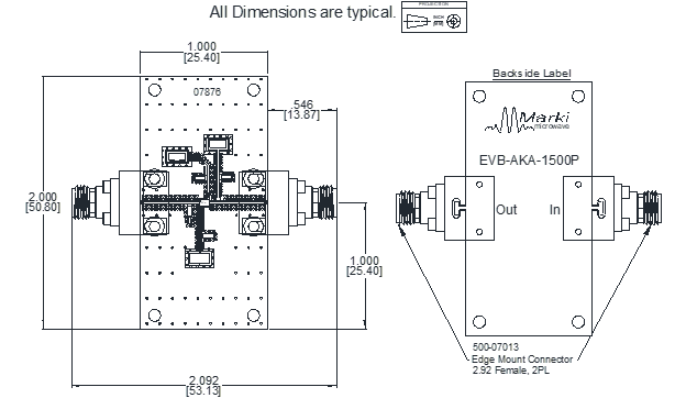
| EVB-AKA-1500P | Evaluation Board, Broadband InGaP SMT DC – 14 GHz Amplifier | EVB | REACH RoHS | Released | EAR99 |
| Part Number | Description | Package | Green Status | Product Lifecycle | Export Classification |
|---|---|---|---|---|---|
| AKA-1500PSM | DC – 14 GHz Broadband InGaP SMT Amplifier | DFN | REACH RoHS | Released | EAR99 |
| EVB-AKA-1500P | Evaluation Board, Broadband InGaP SMT DC – 14 GHz Amplifier | EVB | REACH RoHS | Released | EAR99 |
AKA-1500PSM
DC – 14 GHz Broadband InGaP SMT Amplifier
| Revision Code | Revision Date | Comment |
|---|---|---|
| - | 2023-04-01 | Datasheet Initial Release |
AKA-1500PSM
DC – 14 GHz Broadband InGaP SMT Amplifier
A port diagram of the AKA-1500PSM is shown below.
| Port | Function | Description | DC Equivalent Circuit |
|---|---|---|---|
| 1, 3, 4, 6 | N/C | These pins are internally no-connects and should be connected to DC/RF ground. |  |
| 2 | RF Input | This is the RF Input port of the amplifier die. It is RF matched to 50 Ω and requires an external DC blocking capacitor. |  |
| 5 | RF Output and Positive Collector Voltage Supply | This is the RF Output and positive supply voltage port Vc. It is RF matched to 50 Ω and is DC coupled. An external bias tee is required on this port. | |
| Paddle | Ground | Package ground paddle must be connected to a DC/RF ground potential with high thermal and electrical conductivity. | |
AKA-1500PSM
DC – 14 GHz Broadband InGaP SMT Amplifier
The Absolute Maximum Ratings indicate limits beyond which damage may occur to the device. If these limits are exceeded, the device may become inoperable or have a reduced lifetime.
| Parameter | Maximum Rating | Unit |
|---|---|---|
| Maximum Operating Temperature | 85 | °C |
| Maximum Storage Temperature | 150 | °C |
| Max Junction Temperature for MTTF > 1E6 Hours | 150 | °C |
| Minimum Operating Temperature | -40 | °C |
| Minimum Storage Temperature | -65 | °C |
| Positive Bias Current (Icc) | 74 | mA |
| Power Dissipation | 308 | mW |
| RF Input Power | 10 | dBm |
| θ_Jc, Junction to Case Thermal Resistance | 212 | ºC/W |
| Parameter | Details | Rating |
|---|---|---|
| ESD | 250 to < 500 Volts | HBM Class 1A |
| Weight | Package name: DFN | 0.007g |
| Dimensions | - | 2.00 x 1.30 mm |
| Moisture Sensitivity Level | - | MSL 1 |
The Recommended Operating Conditions indicate the limits, inside which the device should be operated, to guarantee the performance given in Electrical Specifications. Operating outside these limits may not necessarily cause damage to the device, but the performance may degrade outside the limits of the electrical specifications. For limits, above which damage may occur, see Absolute Maximum Ratings.
| Parameter | Min | Nominal | Max | Unit |
|---|---|---|---|---|
| Ambient Temperature | -40 | 25 | 85 | °C |
| Positive DC Device Voltage (Vd) | 4.1 | 4.2 | 4.3 | V |
| Positive DC Current (Icc) | 35 | 50 | 60 | mA |
AKA-1500PSM
DC – 14 GHz Broadband InGaP SMT Amplifier
Unless otherwise specified, electrical specifications apply at TA=+25°C, Vc = +4.2V in a 50Ω system. Typical performance data is measured from EVB unless otherwise stated. Min and Max limits are guaranteed at TA=+25°C.
| Parameter | Test Conditions | Minimum Frequency (GHz) | Maximum Frequency (GHz) | Min | Typ | Max | Unit |
|---|---|---|---|---|---|---|---|
| Small Signal Gain | Vc = +4.2 V, Icc = 50 mA | 0.1 | 4 | 17 | 19 | - | dB |
| Small Signal Gain | Vc = +4.2 V, Icc = 50 mA | 4 | 6 | 15 | 17 | - | dB |
| Small Signal Gain | Vc = +4.2 V, Icc = 50 mA | 6 | 12 | 9 | 13 | - | dB |
| Small Signal Gain | Vc = +4.2 V, Icc = 50 mA | 12 | 14 | 7 | 9 | - | dB |
| Output P1dB | Vc = +4.2 V, Icc = 50 mA | 2 | 6 | 14 | 16 | - | dBm |
| Output P1dB | Vc = +4.2 V, Icc = 50 mA | 6 | 14 | 11 | 13 | - | dBm |
| Input Return Loss | Vc = +4.2 V, Icc = 50 mA | 0.1 | 14 | - | 14 | - | dB |
| Output Return Loss | Vc = +4.2 V, Icc = 50 mA | 0.1 | 14 | - | 22 | - | dB |
| Reverse Isolation | Vc = +4.2 V, Icc = 50 mA | 0.1 | 14 | - | 19 | - | dB |
| Noise Figure | Vc = +4.2 V, Icc = 50 mA | 0.1 | 6 | - | 4 | - | dB |
| Noise Figure | Vc = +4.2 V, Icc = 50 mA | 6 | 14 | - | 5 | - | dB |
| Current Consumption | Vc = +4.2V,
No RF Input
| - | - | - | 50 | - | mA |
| Output IP3 | Vc = +4.2 V, Icc = 50 mA | 0.1 | 6 | - | 28 | - | dBm |
| Output IP3 | Vc = +4.2 V, Icc = 50 mA | 6 | 14 | - | 26 | - | dBm |
AKA-1500PSM
DC – 14 GHz Broadband InGaP SMT Amplifier


AKA-1500PSM
DC – 14 GHz Broadband InGaP SMT Amplifier


AKA-1500PSM
DC – 14 GHz Broadband InGaP SMT Amplifier

AKA-1500PSM
DC – 14 GHz Broadband InGaP SMT Amplifier
AKA-1500PSM
DC – 14 GHz Broadband InGaP SMT Amplifier
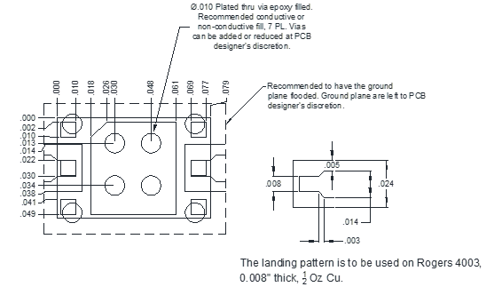
Download : Footprint Drawing
AKA-1500PSM
DC – 14 GHz Broadband InGaP SMT Amplifier