


Absolute Maximum Ratings
The Absolute Maximum Ratings indicate limits beyond which damage may occur to the device. If these limits are exceeded, the device may become inoperable or have a reduced lifetime. Reliability limits are individual, instantaneous catastrophic limits only. Functional operation limits are indicated below. Operation of the device at multiple absolute maximum limits or for extended periods at a single limit can cause degradation and damage to the device
| Parameter | Maximum Rating | Unit |
|---|---|---|
| Bias Current (Ib) | 10 | mA |
| Bias Voltage (Vb) | 6.5 | V |
| Drain Current (Id) (RF Applied) | 120 | mA |
| Drain Supply Voltage (Vd) | 8.5 | V |
| Maximum Operating Temperature for MTTF > 1E6 hours | 85 | °C |
| Maximum Storage Temperature | 125 | °C |
| Minimum Operating Temperature for MTTF > 1E6 hours | -40 | °C |
| Minimum Storage Temperature | -65 | °C |
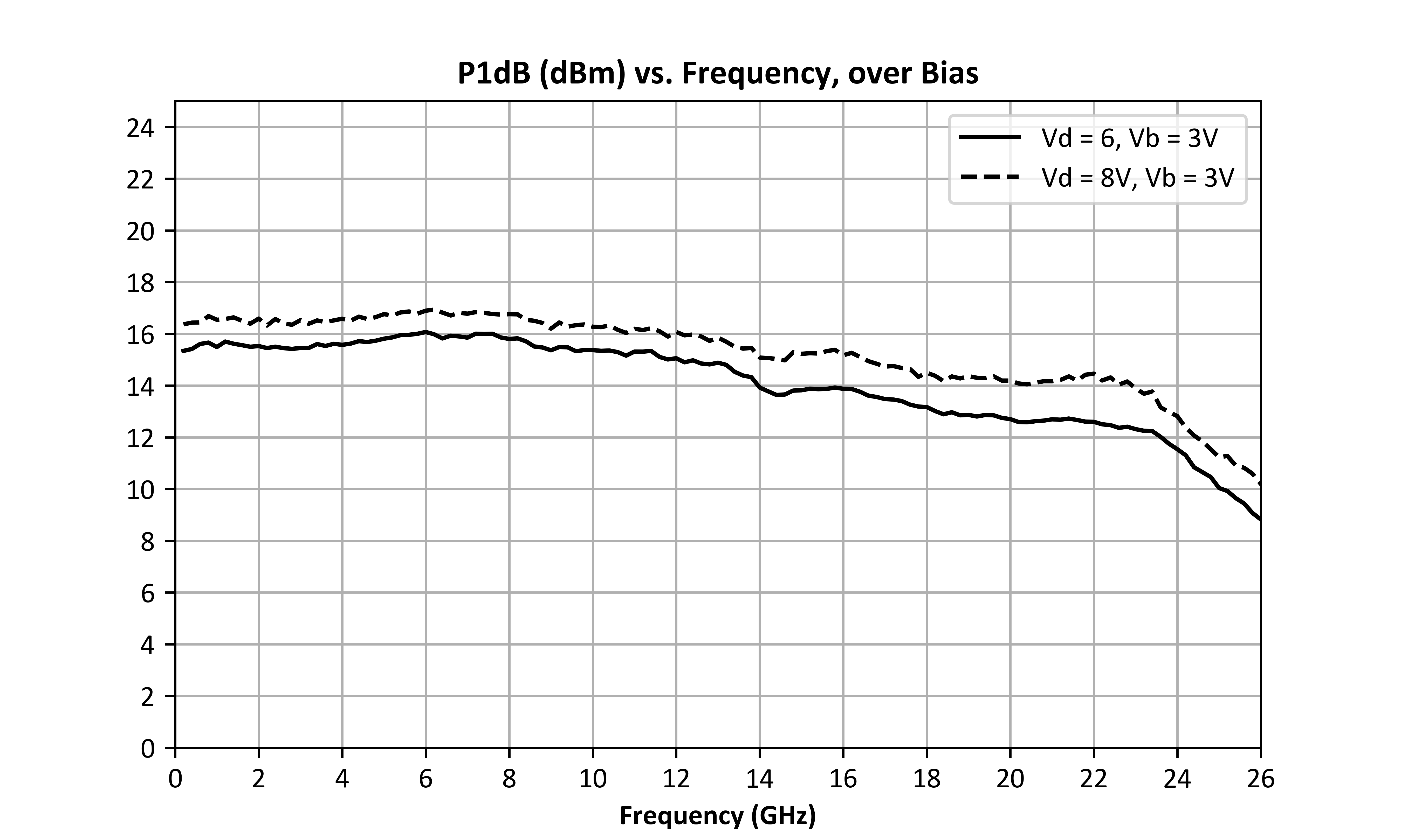
| RF Power Handling | 23 | dBm |
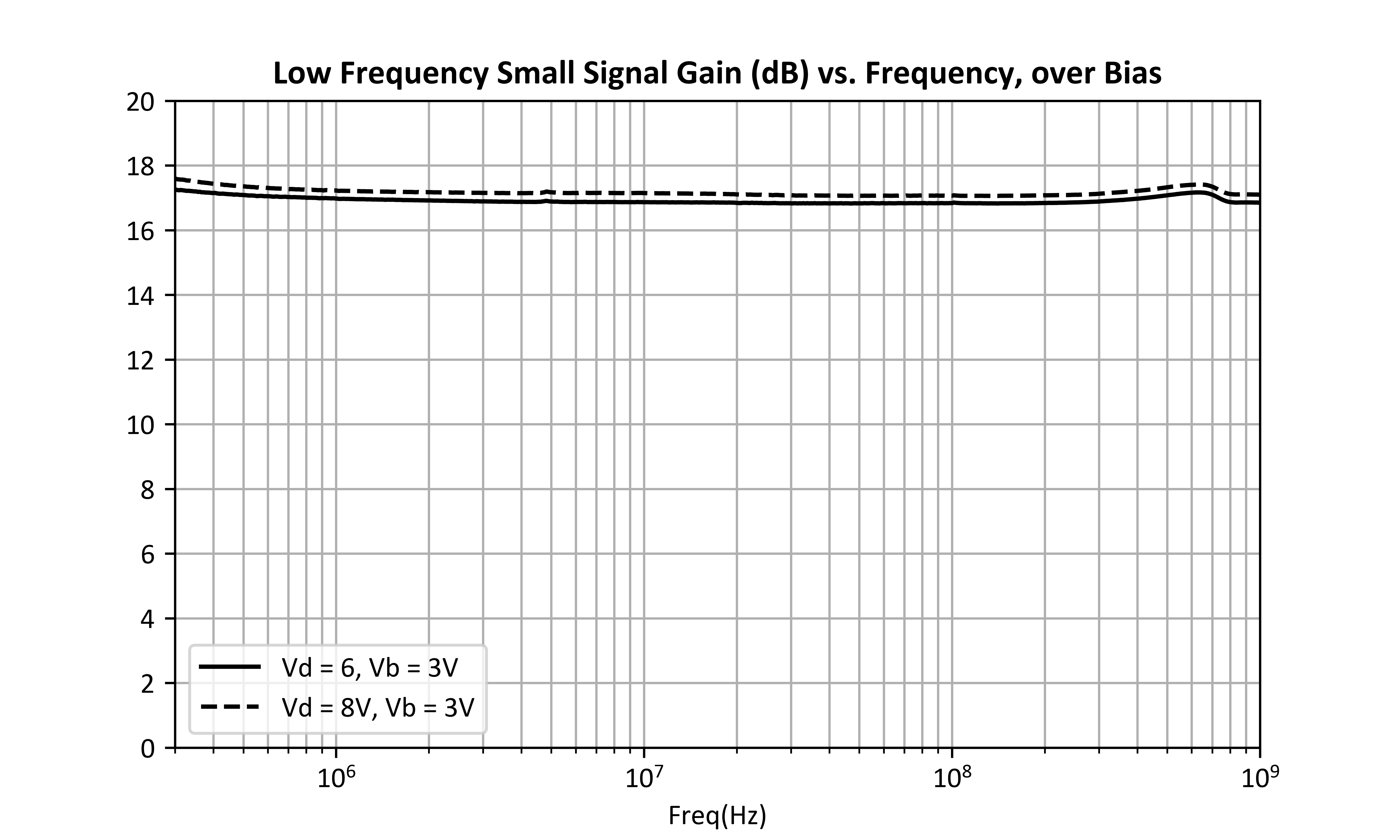
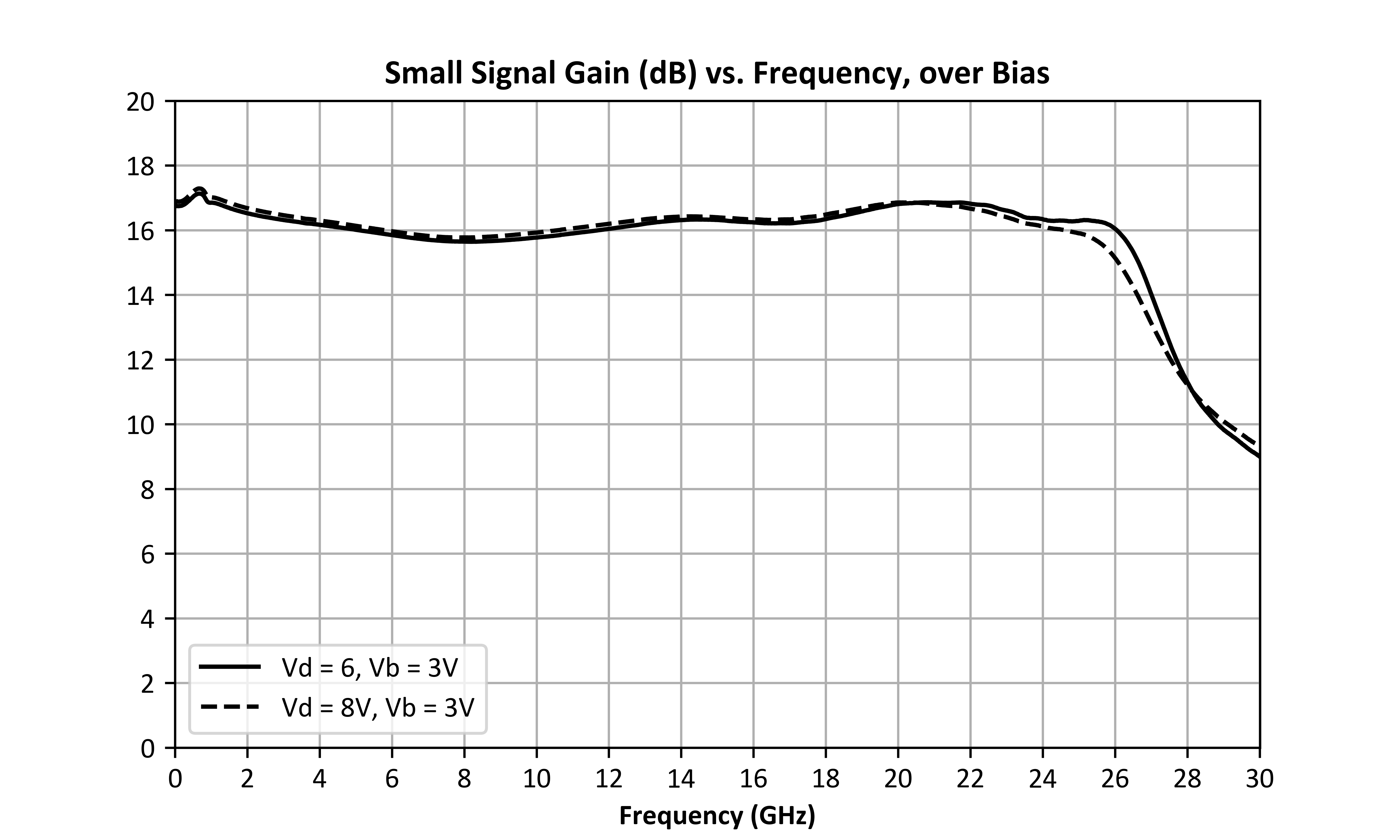%20vs.%20Frequency,%20over%20Bias.png)
%20vs.%20Frequency,%20over%20Bias.png)
%20vs.%20Frequency,%20over%20Bias.png)
%20vs.%20Frequency,%20over%20Bias.png)
%20vs.%20Frequency,%20over%20Bias.png)
%20vs.%20Frequency,%20over%20Bias.png)
%20vs.%20Frequency,%20over%20Bias.png)
%20vs.%20Frequency,%20over%20Bias.png)
%20vs.%20Frequency,%20over%20Bias.png)
%20vs.%20Frequency,%20over%20Bias.png)
%20vs.%20Frequency,%20over%20Bias.png)
%20vs.%20Frequency,%20over%20Bias.png)
%20vs.%20Frequency,%20over%20Bias.png)
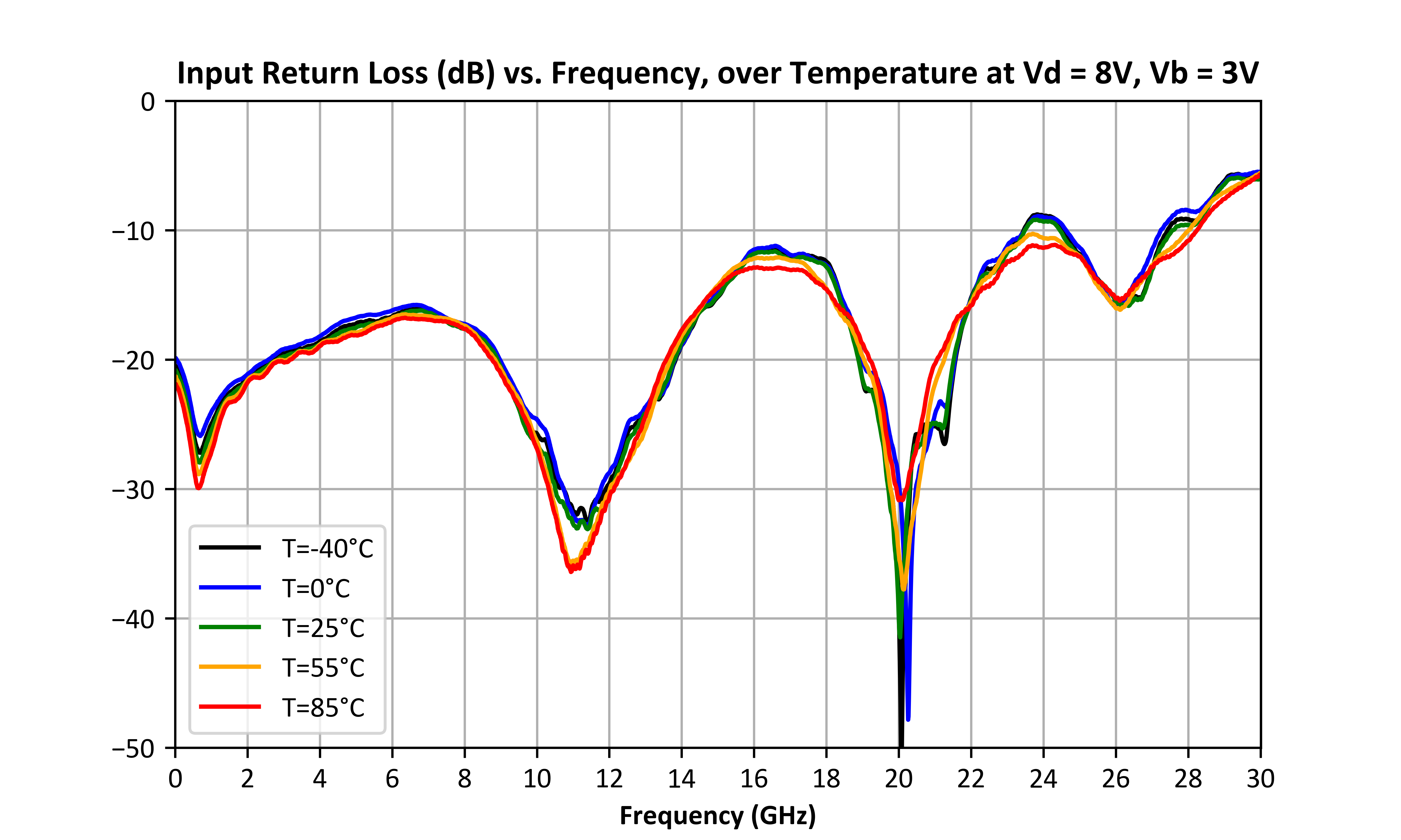
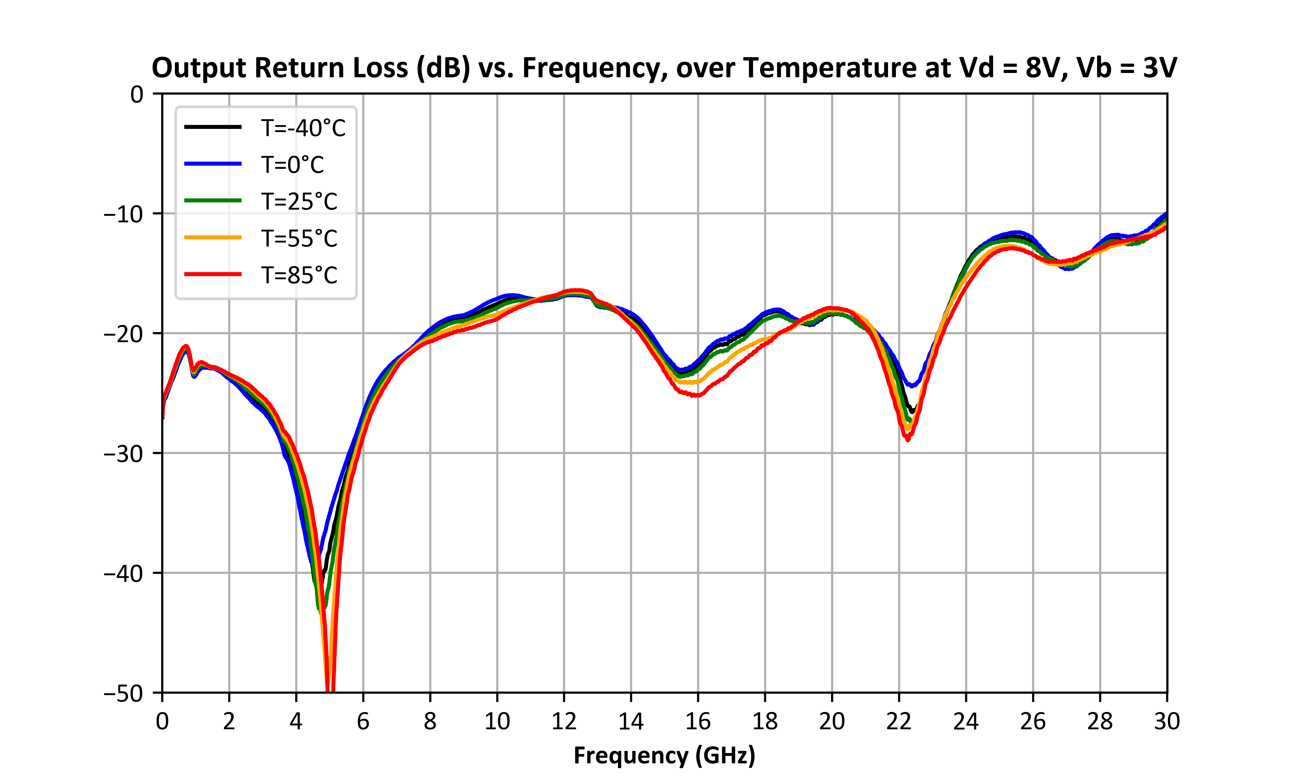
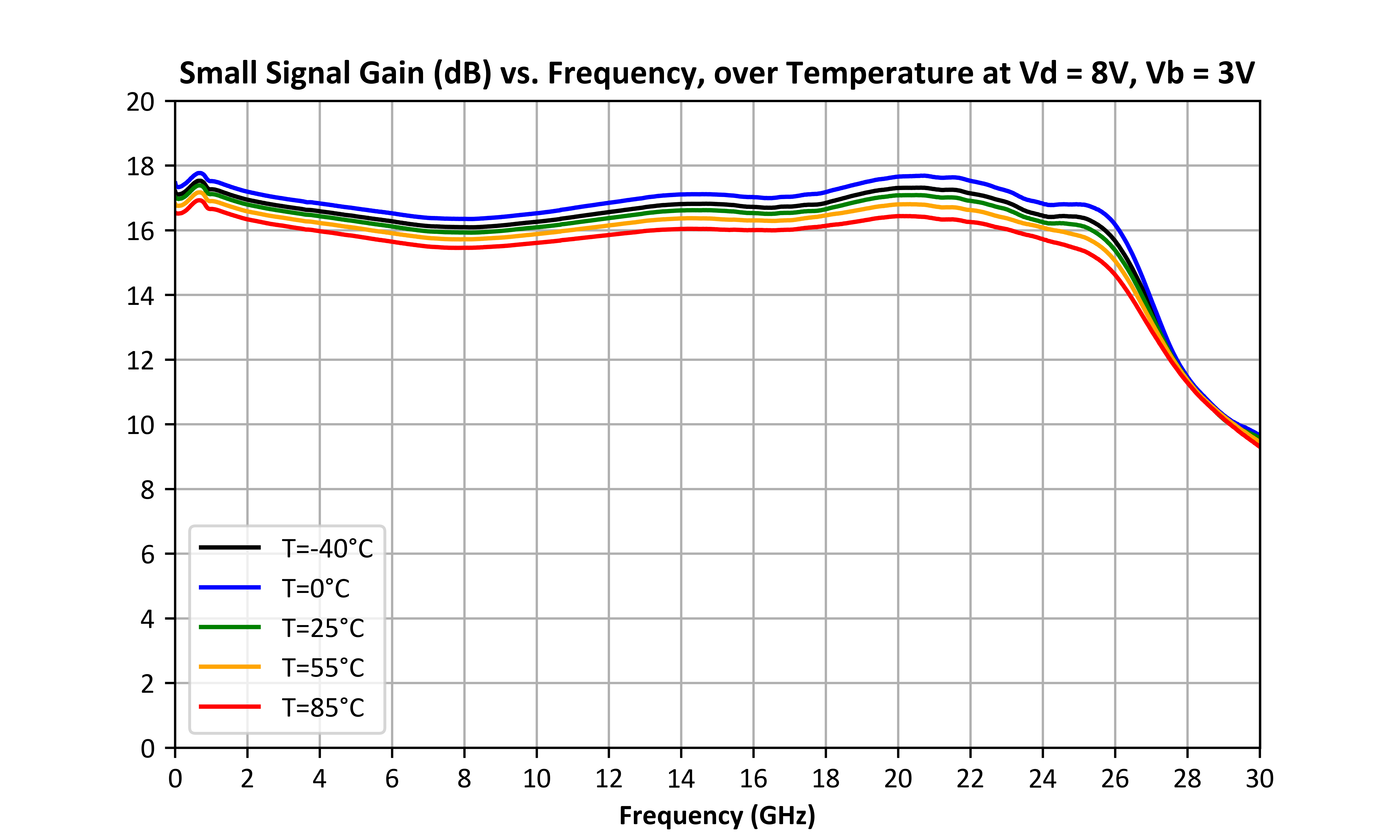
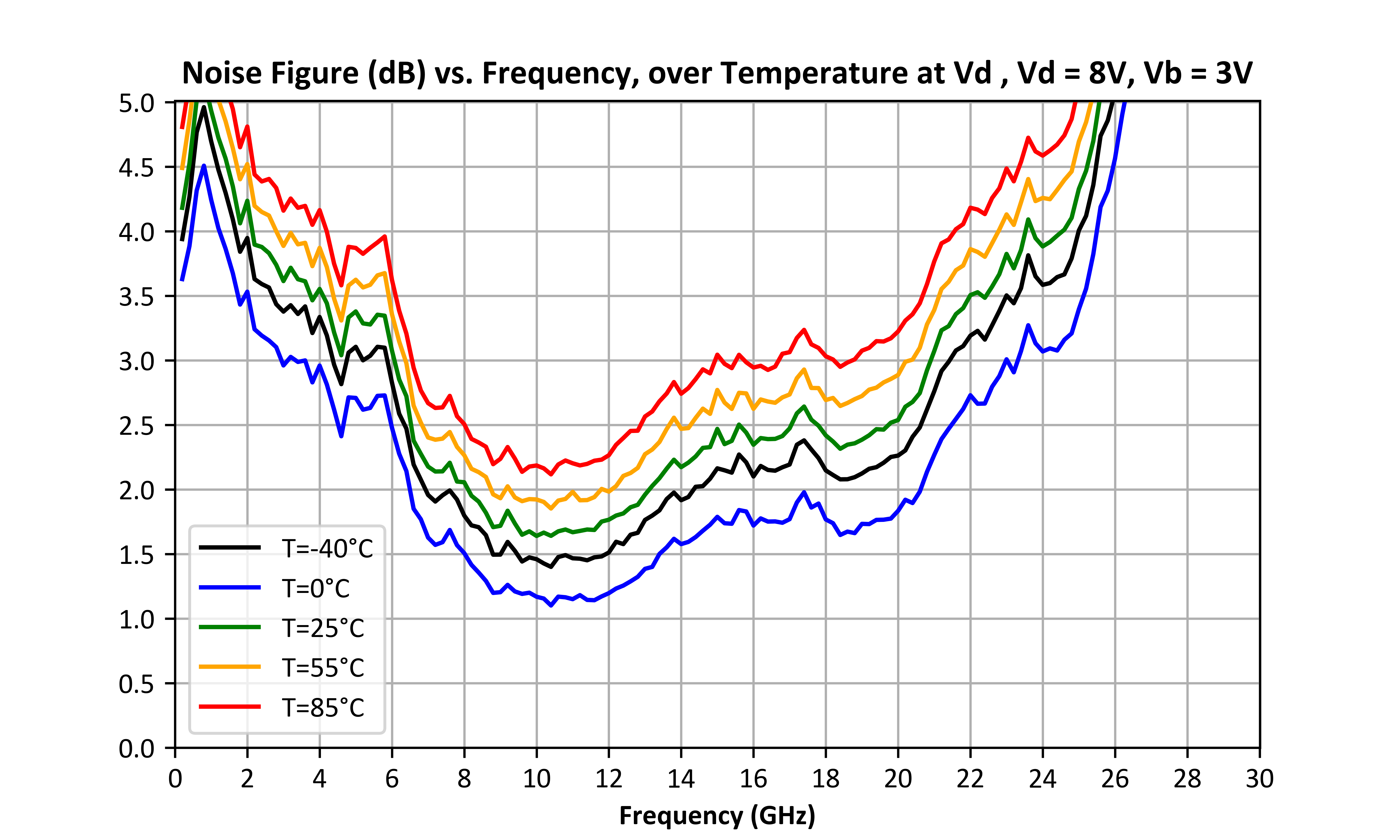
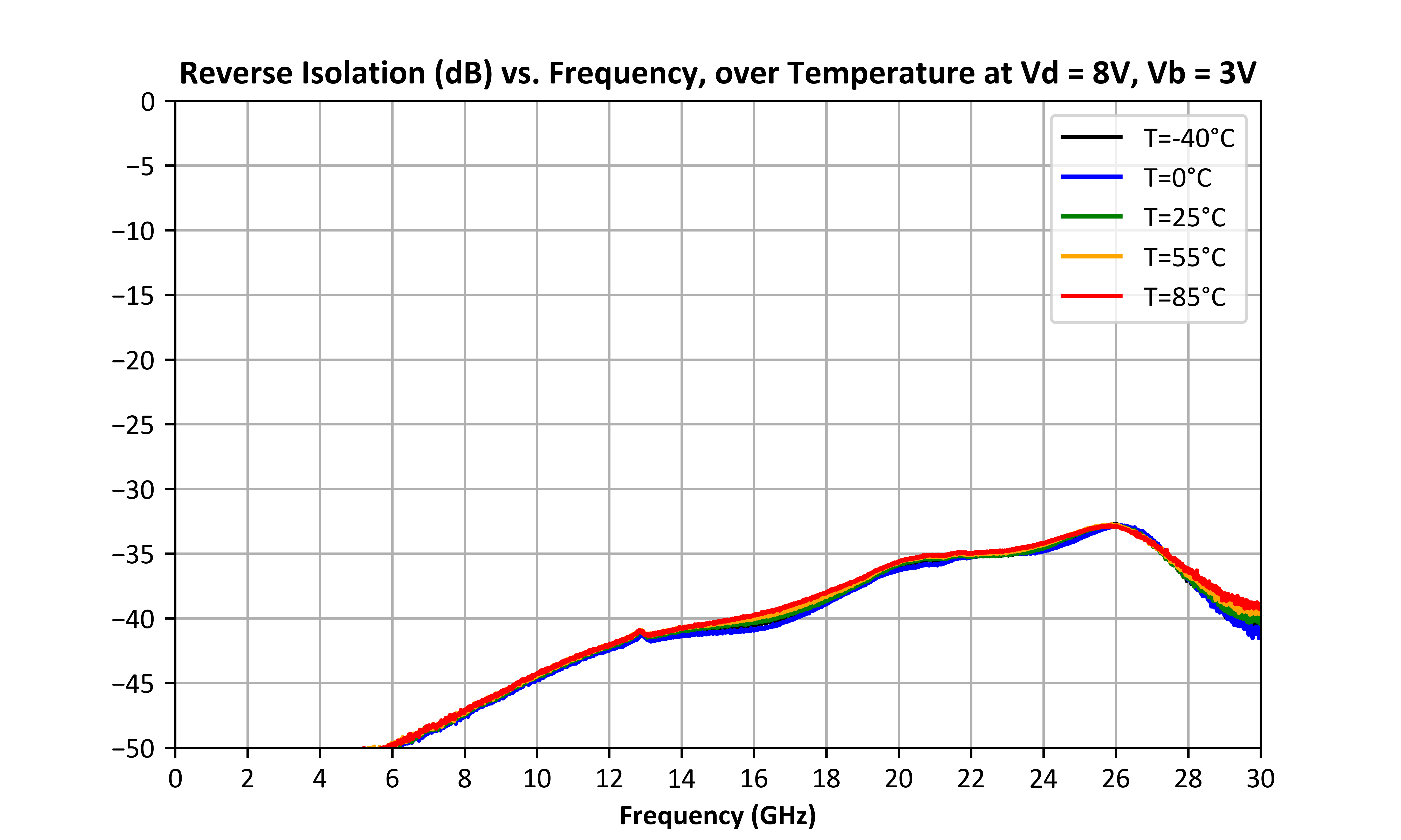
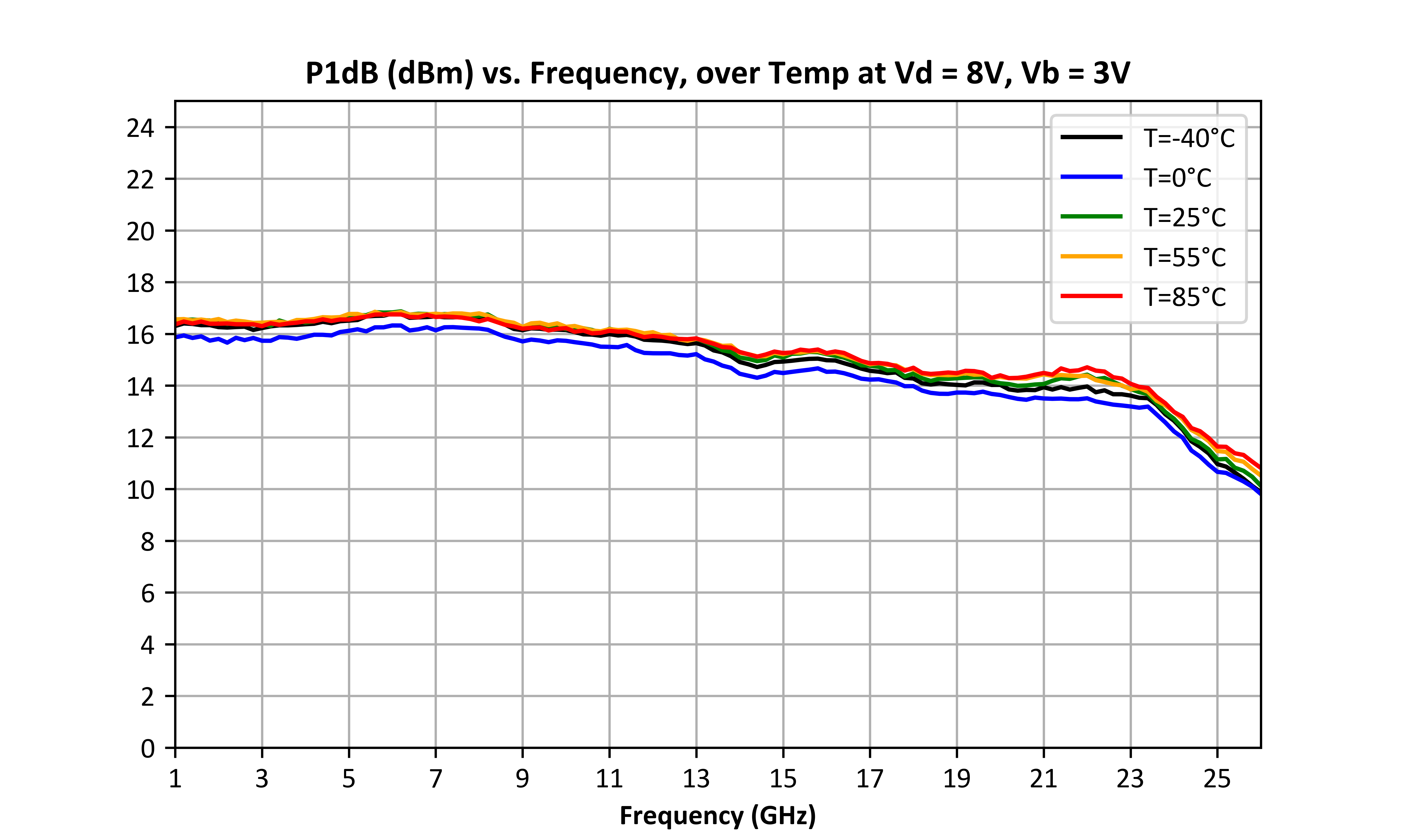%20vs.%20Frequency,%20over%20Temp%20at%20Vd%20=%208V,%20Vb%20=%203V.png)
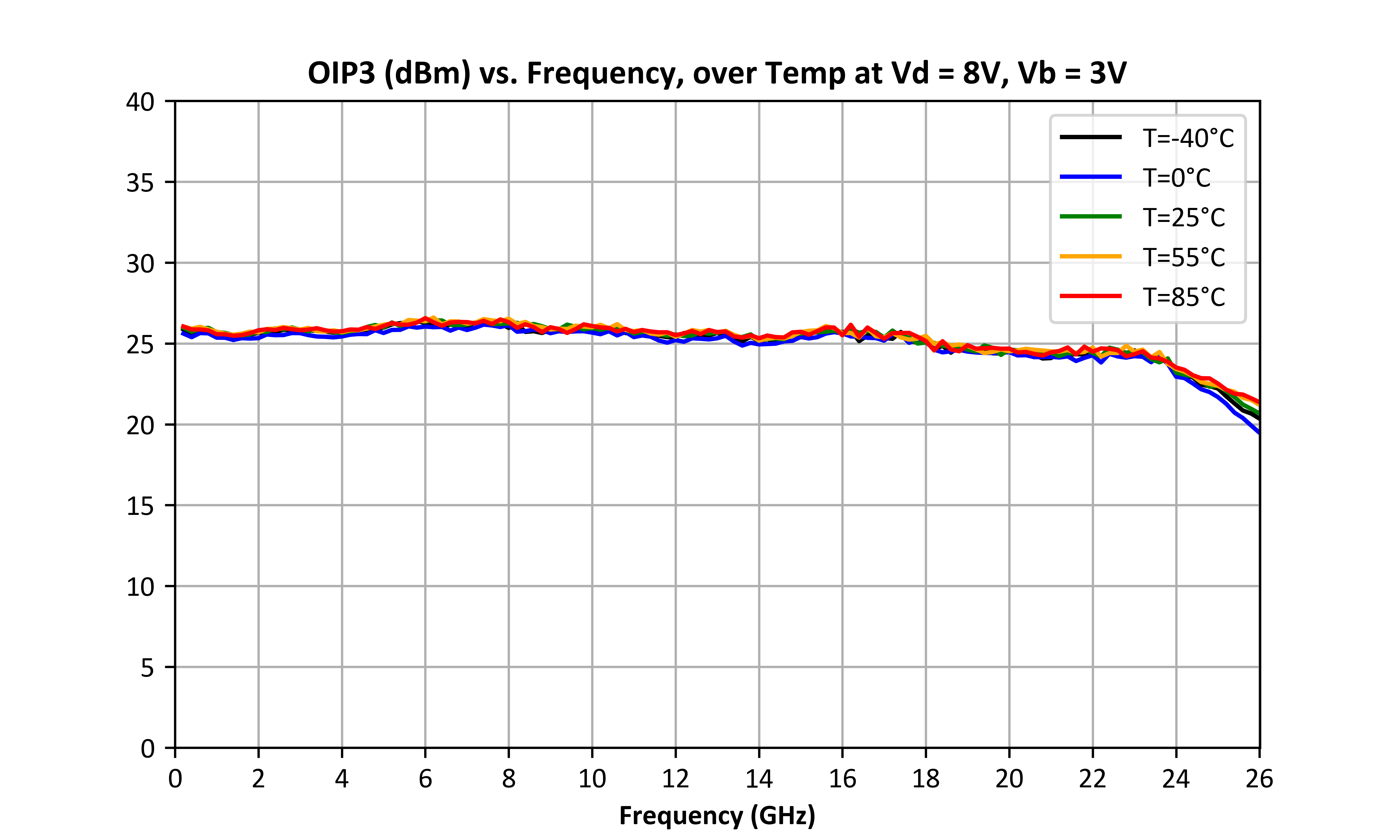%20vs.%20Frequency,%20over%20Temp%20at%20Vd%20=%208V,%20Vb%20=%203V.png)
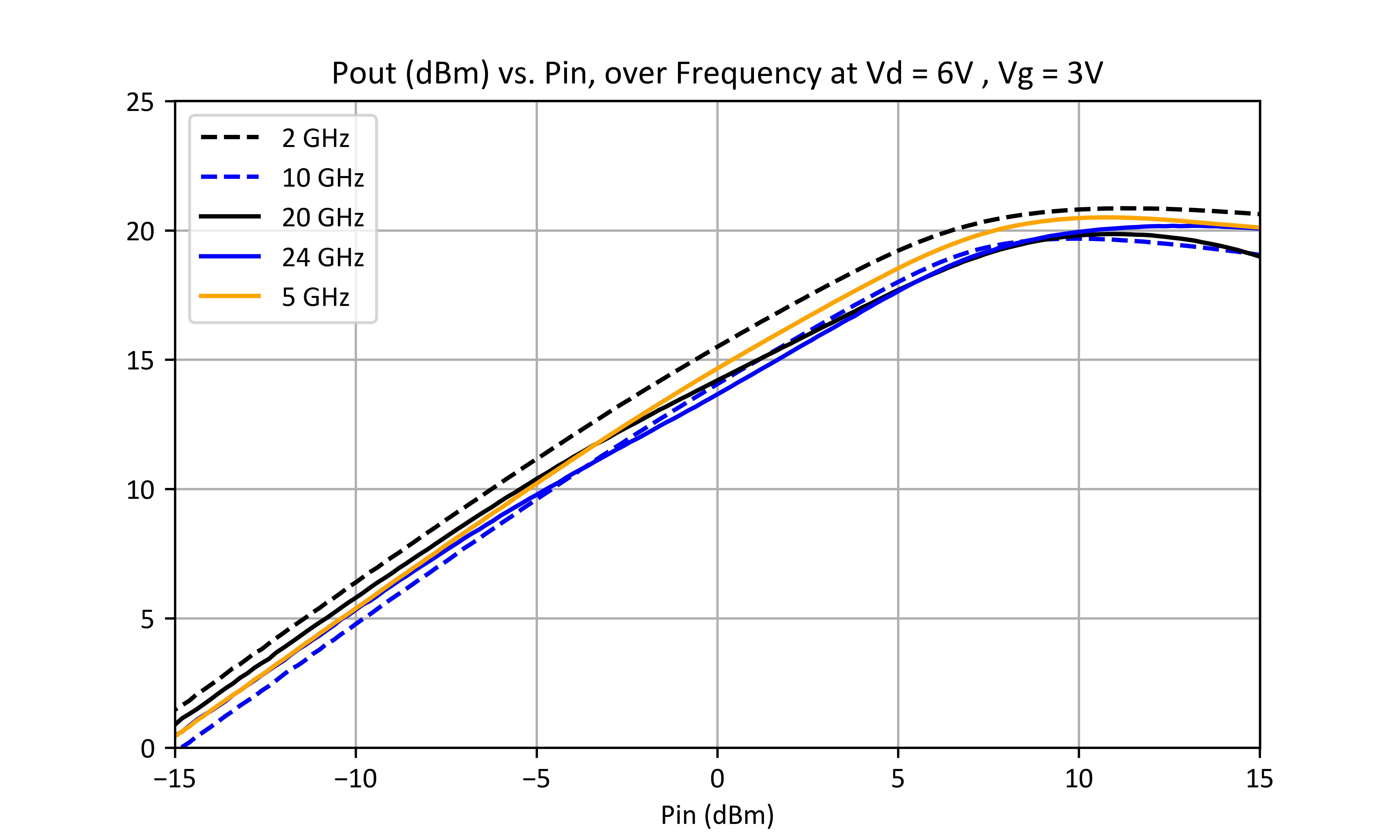%20vs.%20Pin,%20over%20Frequency%20at%20Vd%20=%206V%20,%20Vg%20=%203V.png)
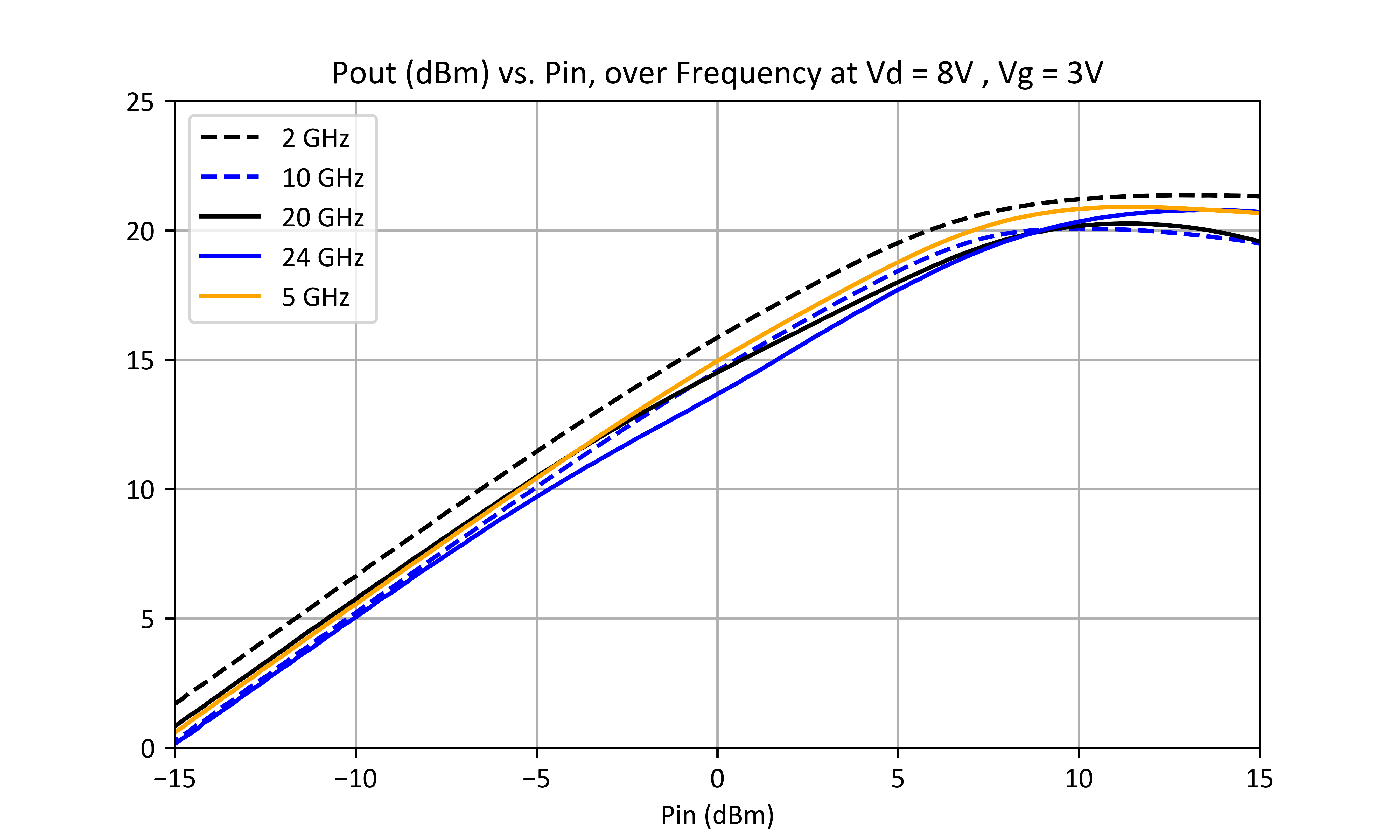%20vs.%20Pin,%20over%20Frequency%20at%20Vd%20=%208V%20,%20Vg%20=%203V.png)
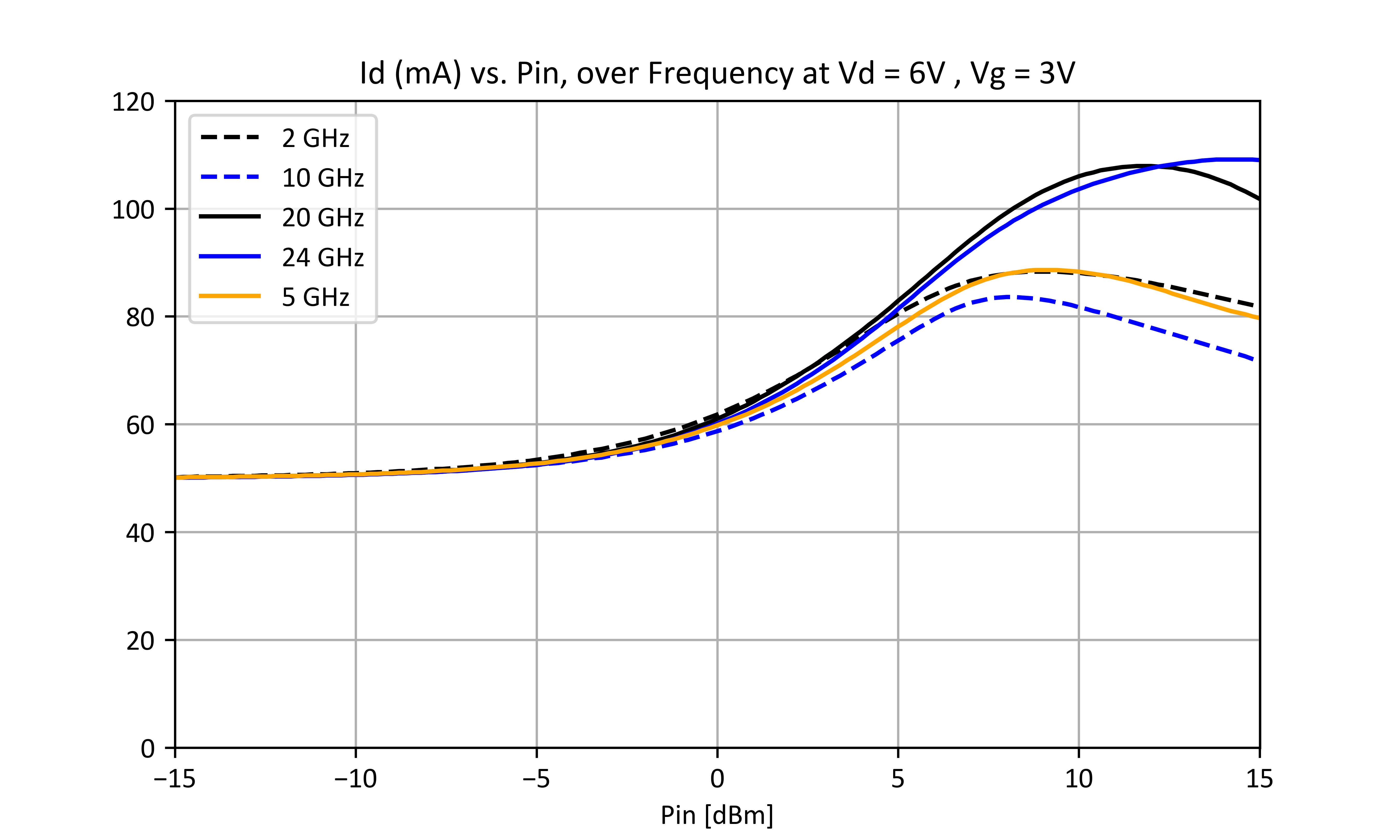%20vs.%20Pin,%20over%20Frequency%20at%20Vd%20=%206V%20,%20Vg%20=%203V.png)
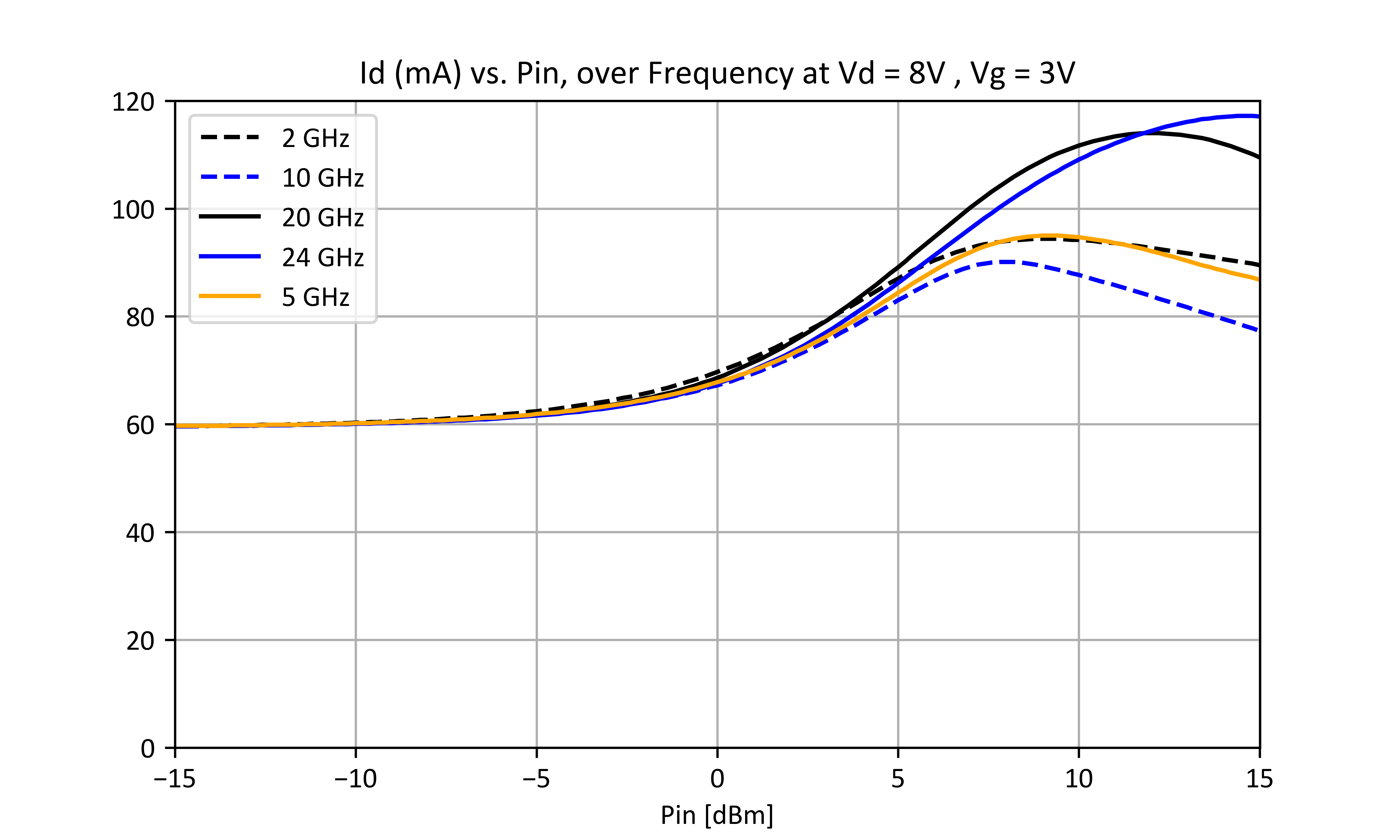%20vs.%20Pin,%20over%20Frequency%20at%20Vd%20=%208V%20,%20Vg%20=%203V.png)
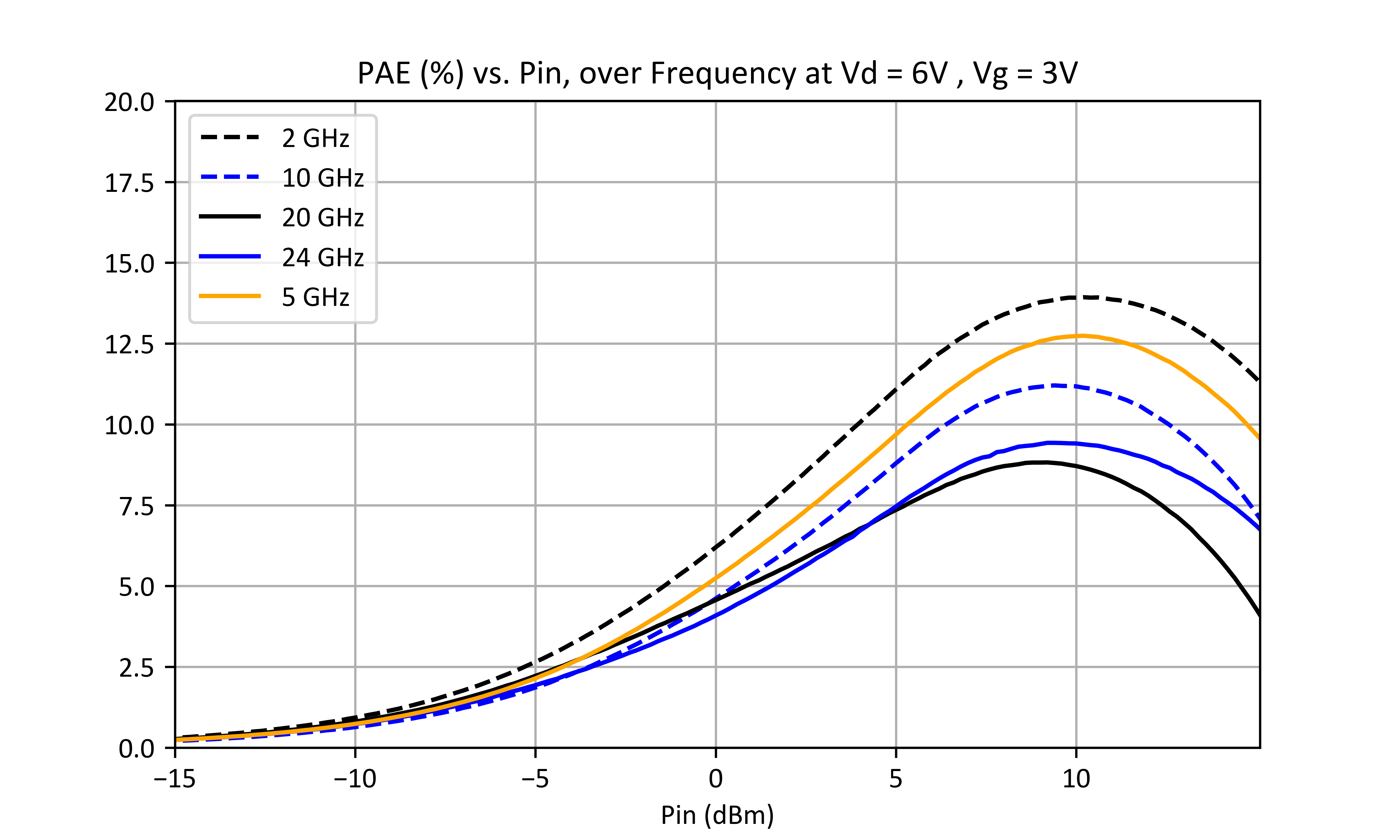%20vs.%20Pin,%20over%20Frequency%20at%20Vd%20=%206V%20,%20Vg%20=%203V.png)
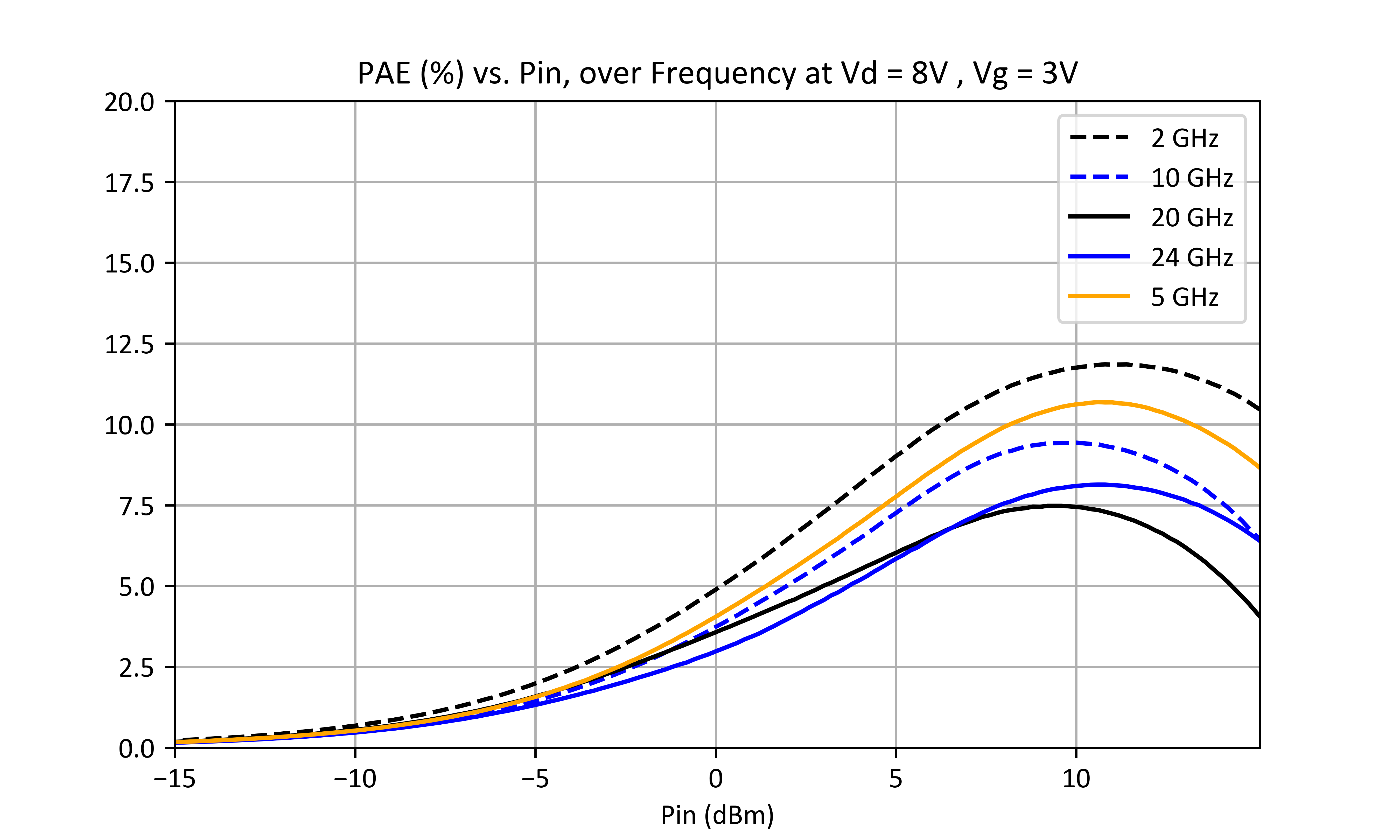%20vs.%20Pin,%20over%20Frequency%20at%20Vd%20=%208V%20,%20Vg%20=%203V.png)