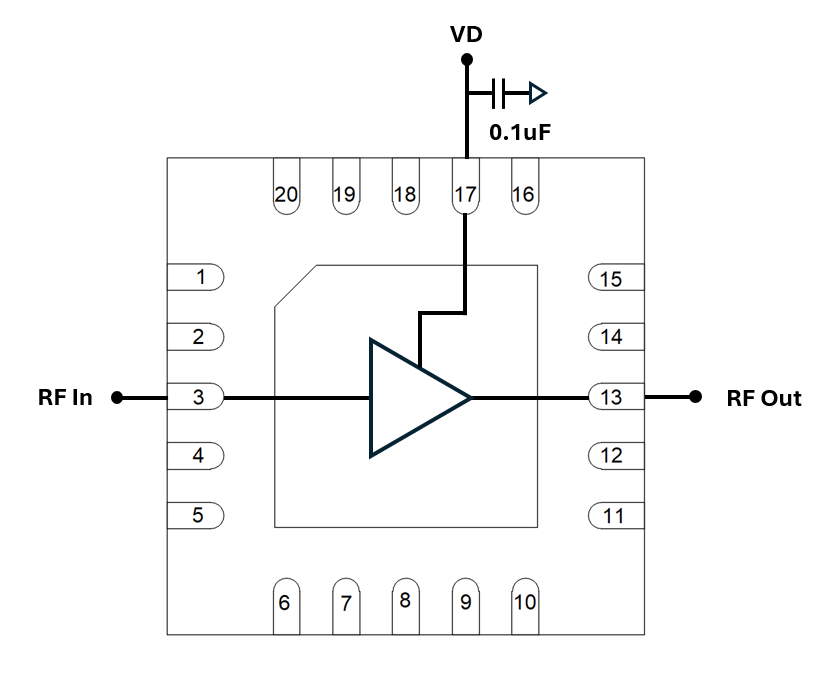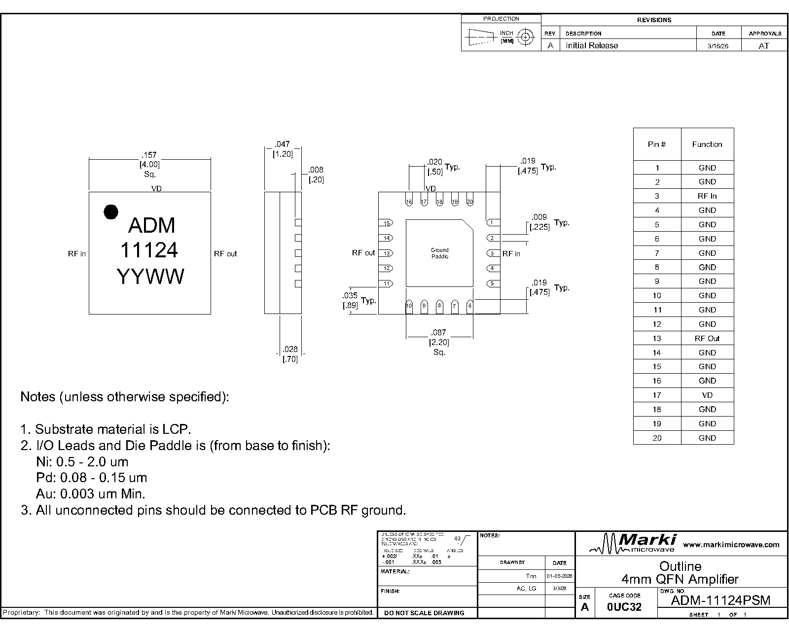
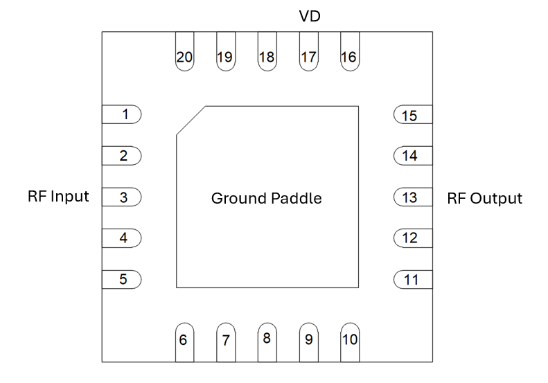
Port Diagram
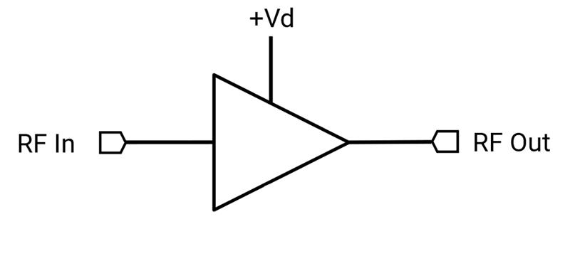
Below is the recommended application circuit for the ADM-11124PSM. This is the configuration that is used to characterize this device. However, each PCB layout and environment are different which may require minor modifications of the biasing network. Please contact [email protected] for more information.


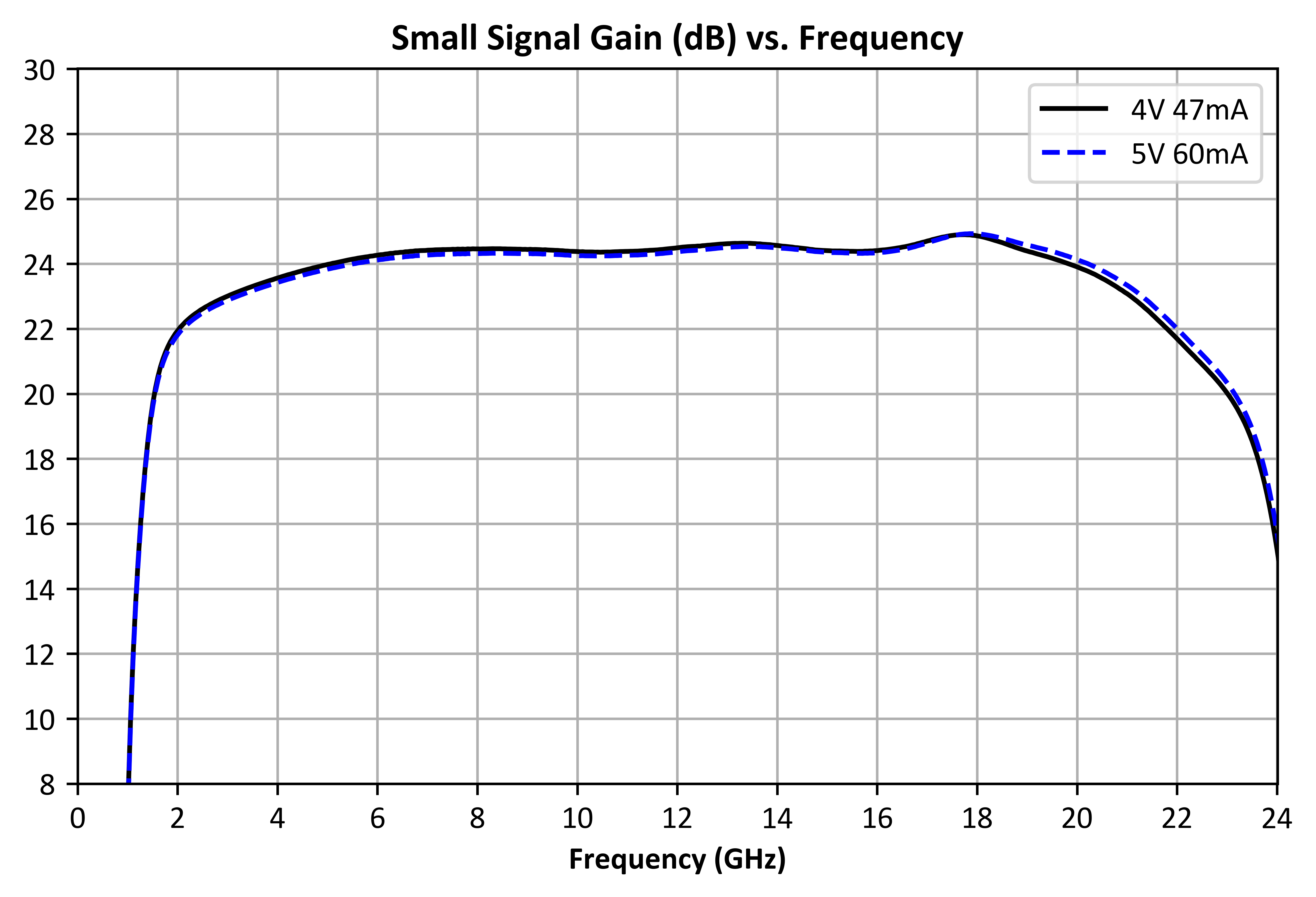%20vs.%20Frequency.png)
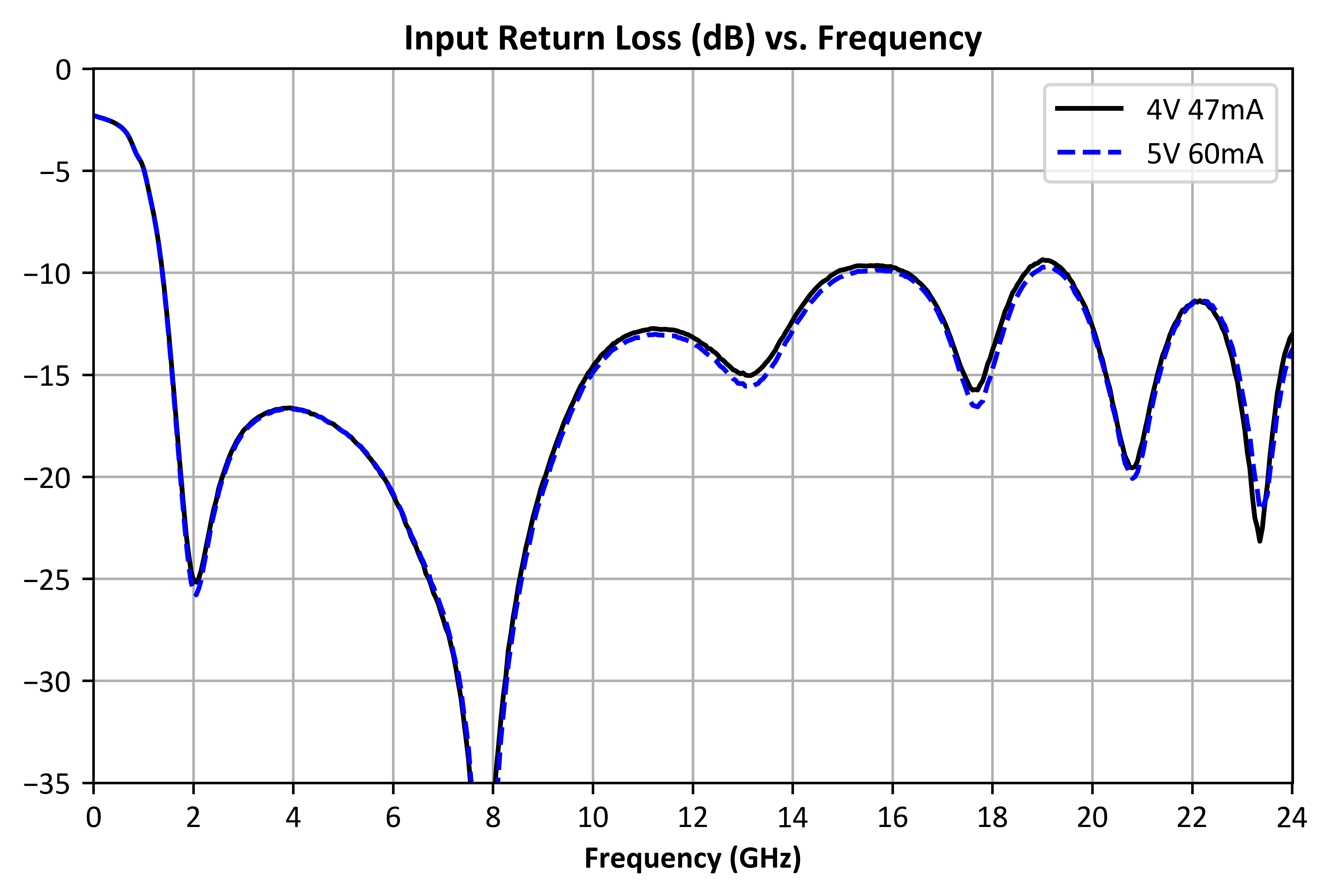%20vs.%20Frequency.png)
%20vs.%20Frequency.png)
%20vs.%20Frequency.png)
%20vs.%20Frequency.png)
%20vs.%20Frequency.png)
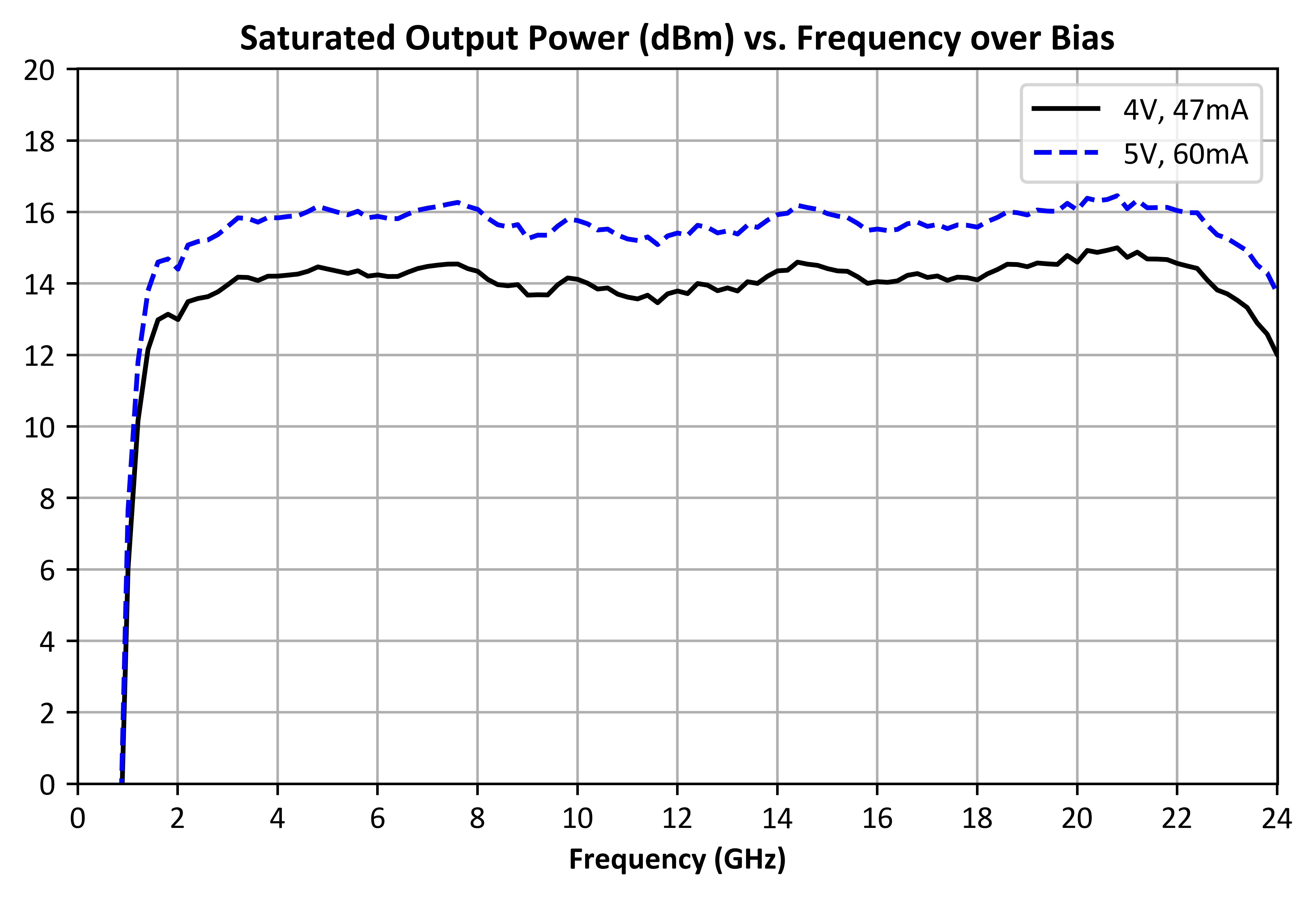%20vs.%20Frequency%20over%20Bias.png)
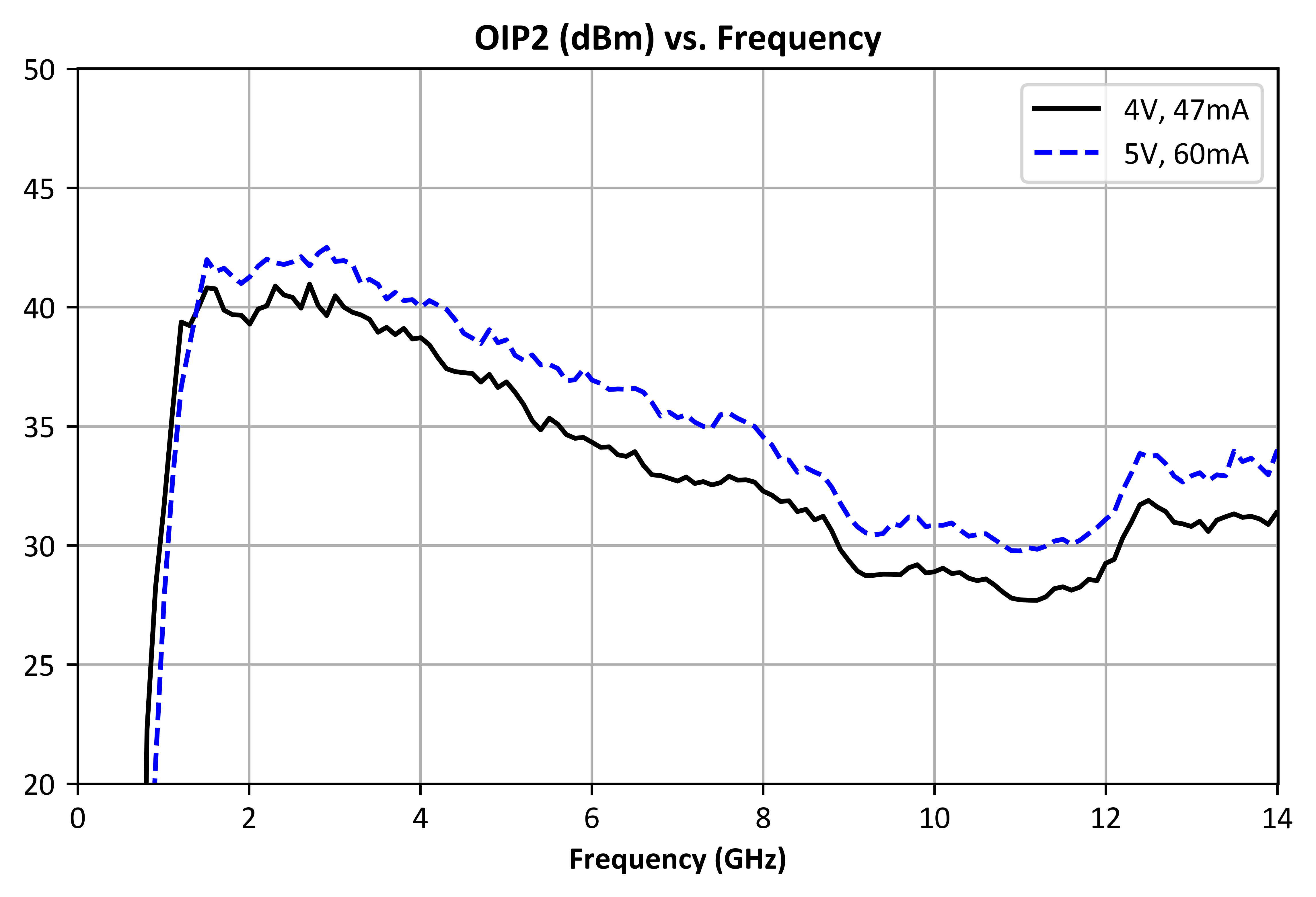%20vs.%20Frequency.png)
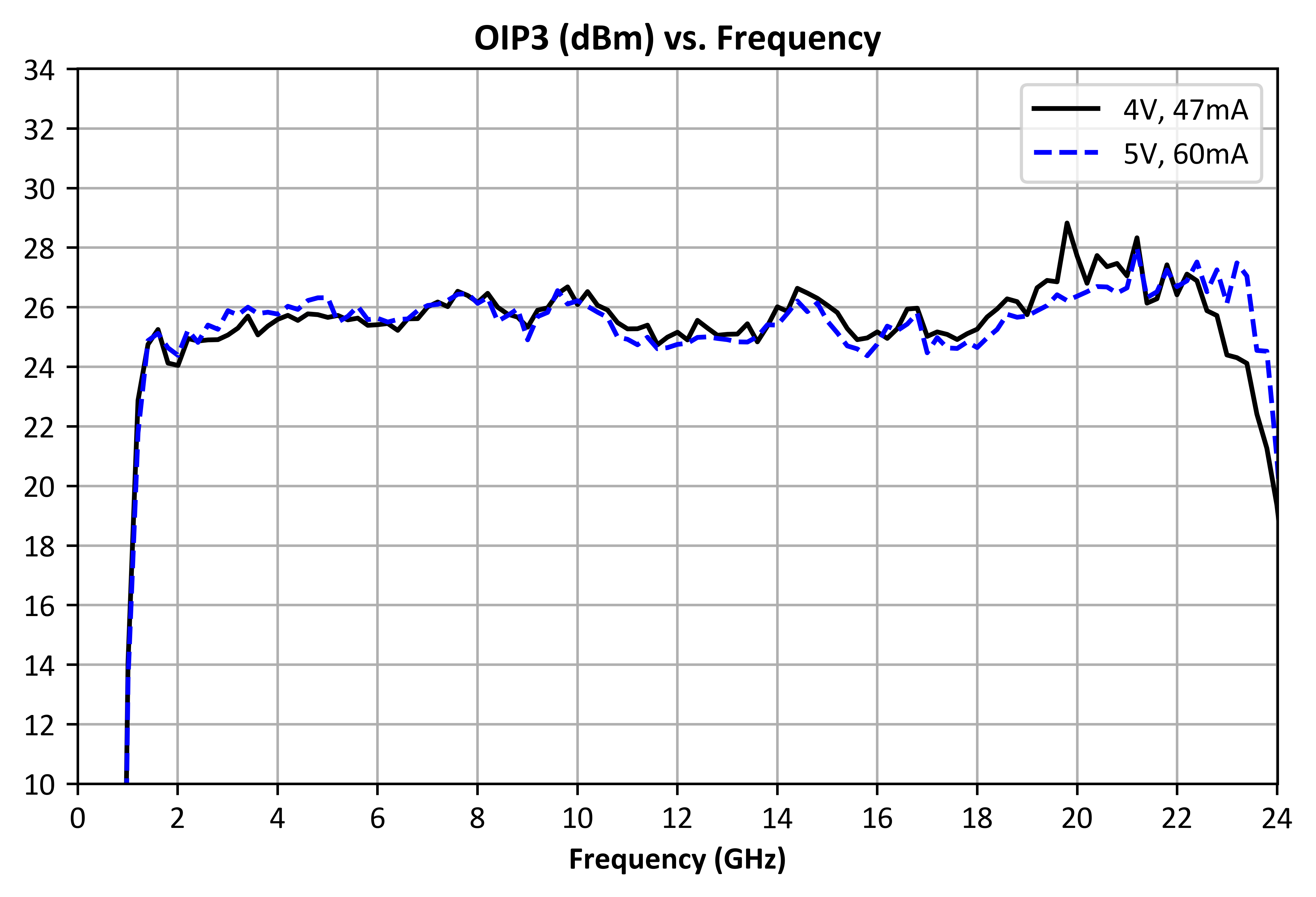%20vs.%20Frequency.png)
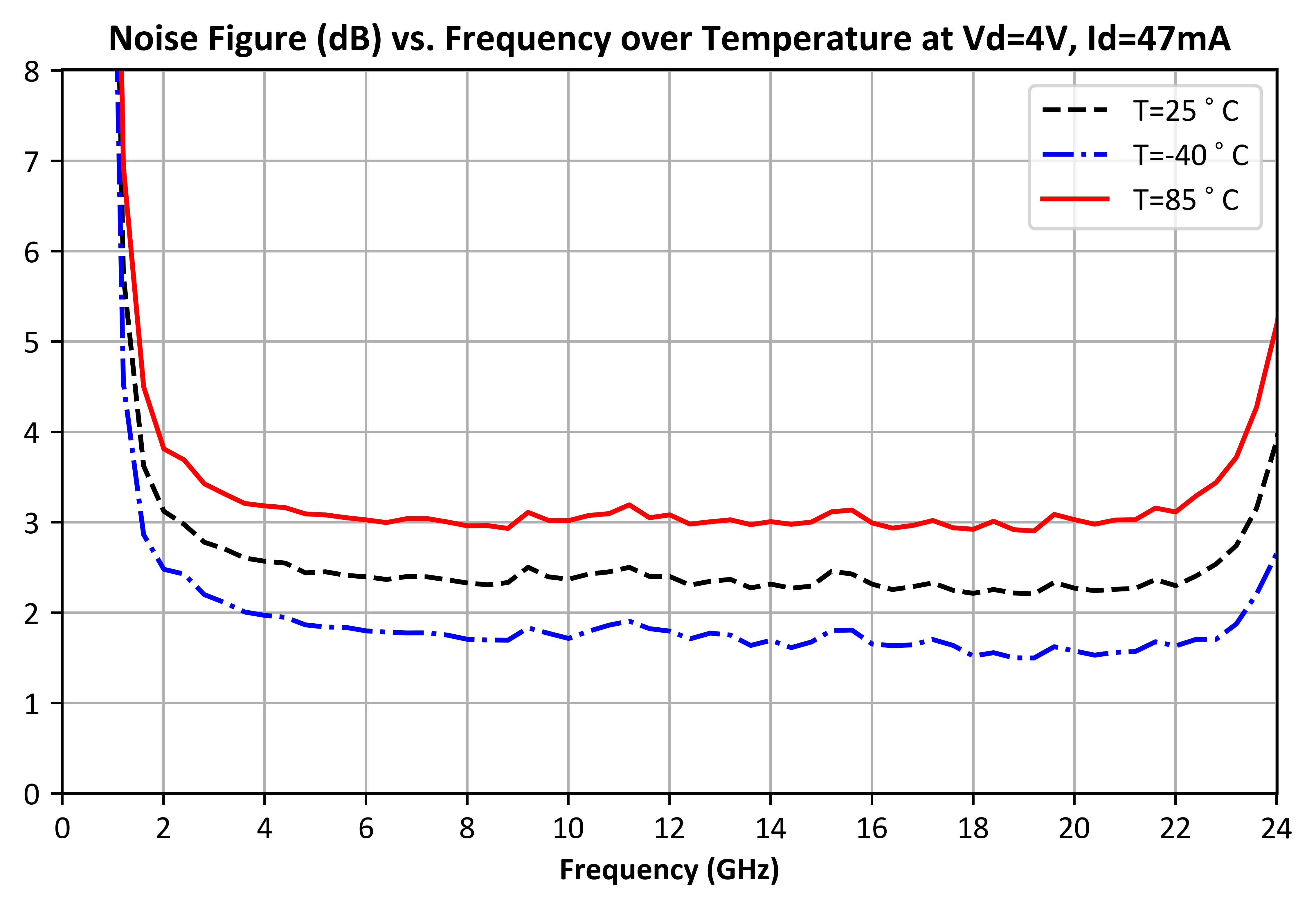
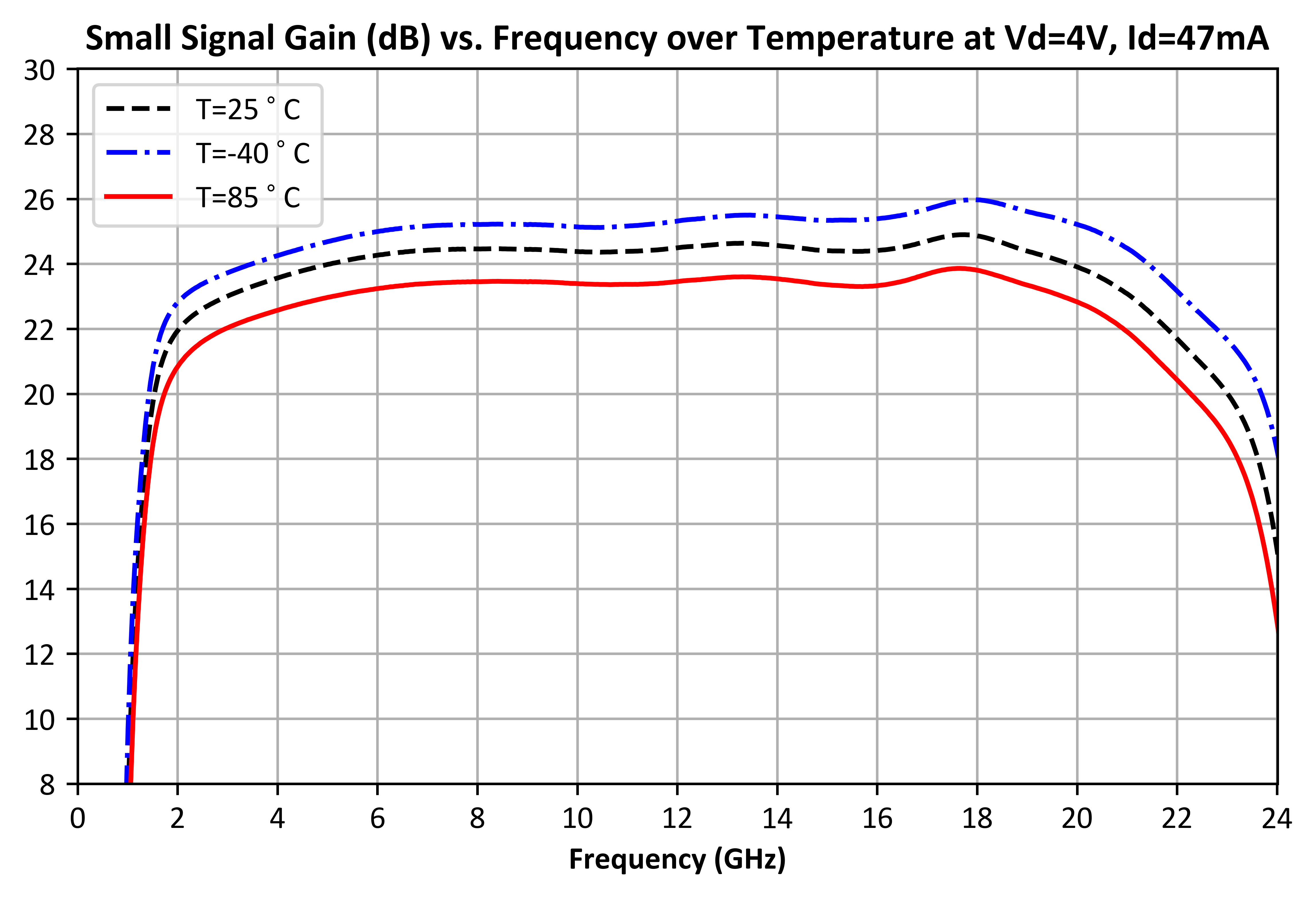%20vs.%20Frequency%20over%20Temperature%20at%20Vd=4V,%20Id=47mA.png)
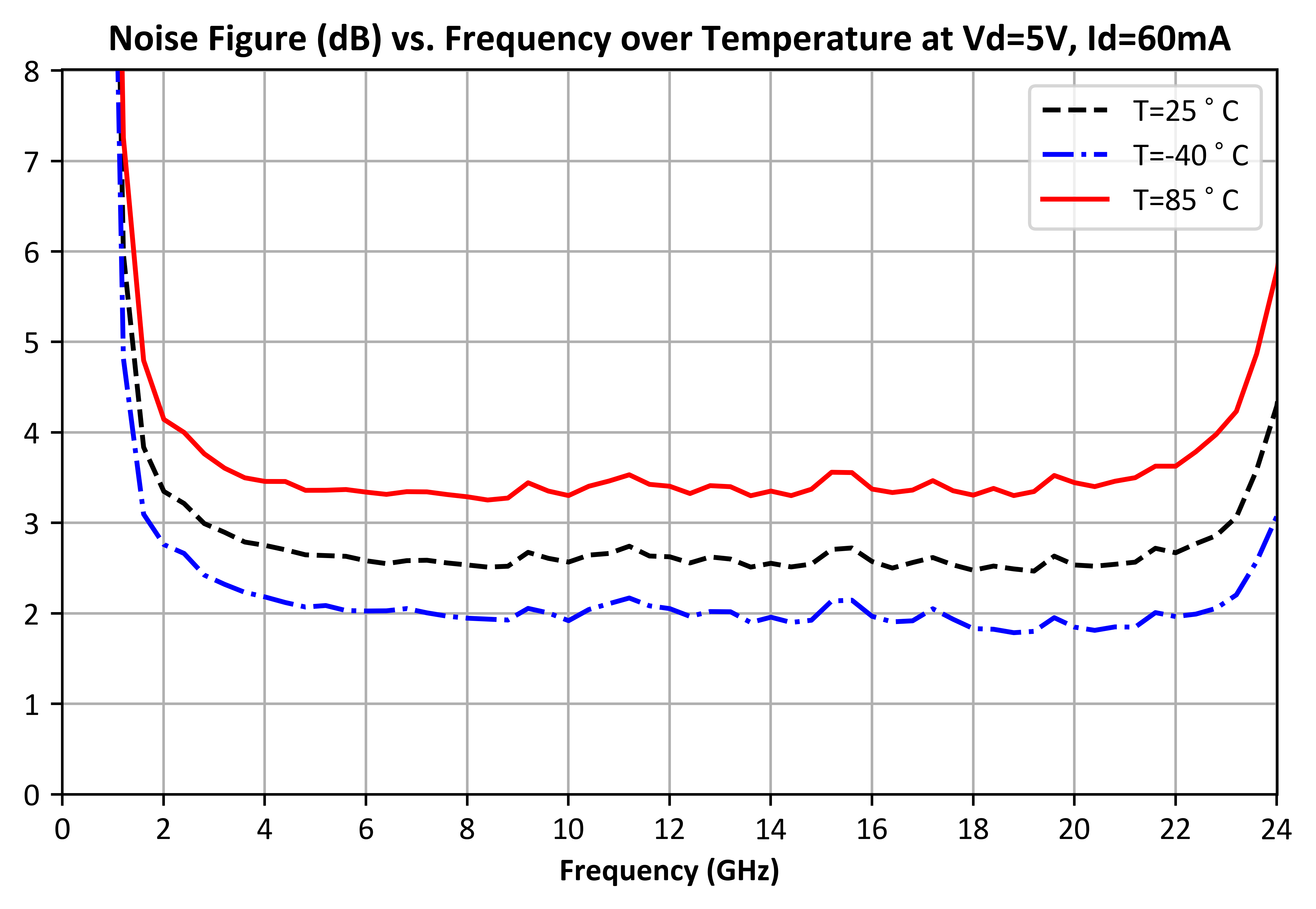
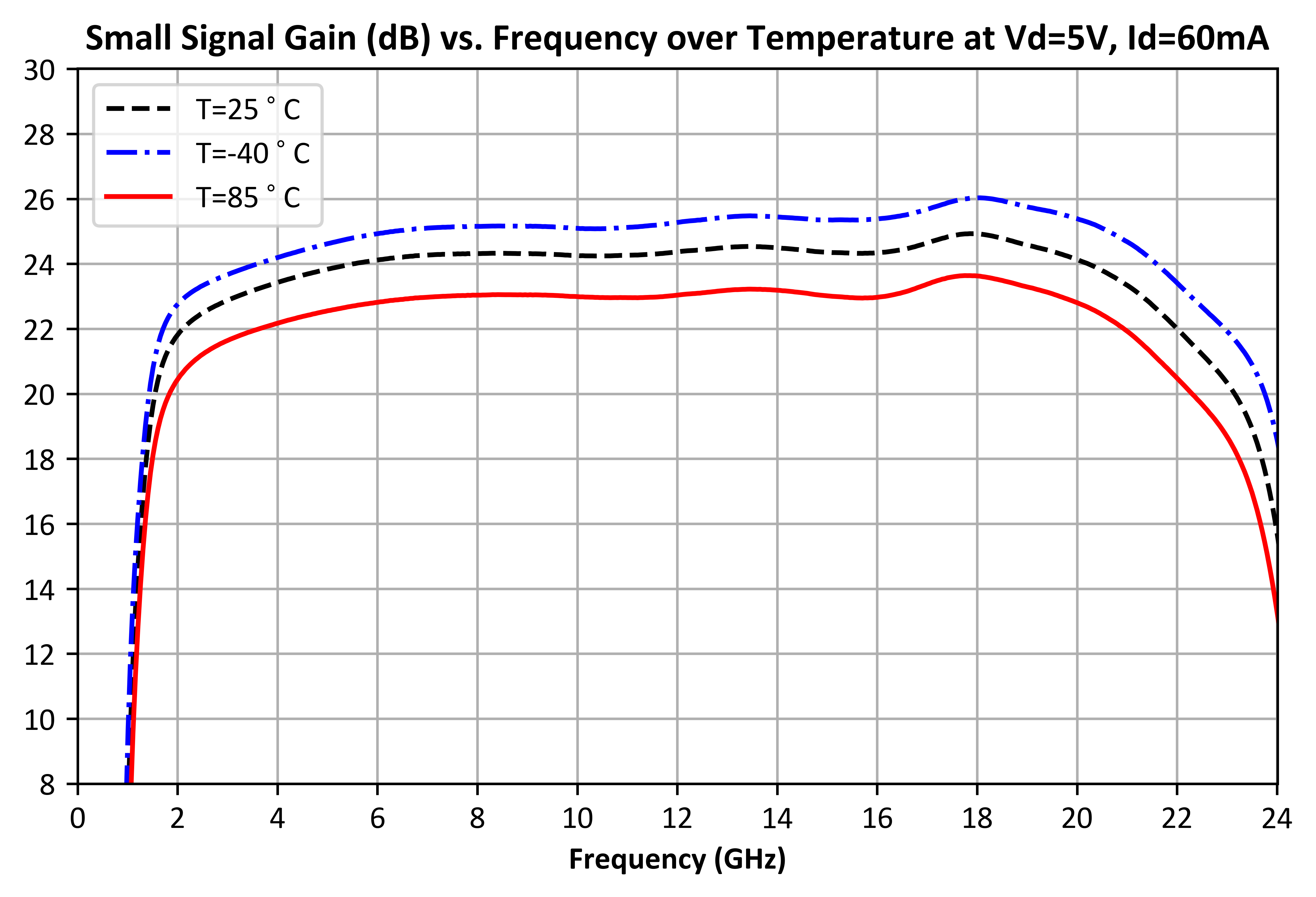%20vs.%20Frequency%20over%20Temperature%20at%20Vd=5V,%20Id=60mA.png)
%20vs.%20Frequency%20over%20Temperature%20at%20Vd=4V,%20Id=47mA.png)
%20vs.%20Frequency%20over%20Temperature%20at%20Vd=5V,%20Id=60mA.png)