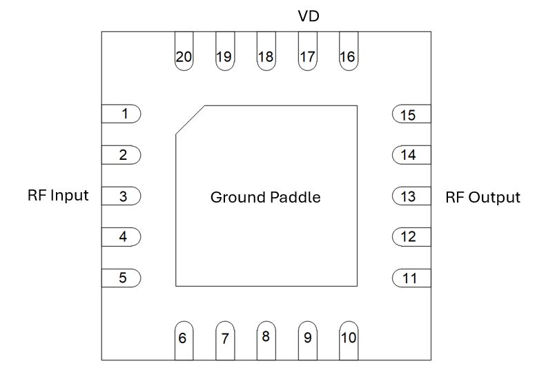
Port Diagram
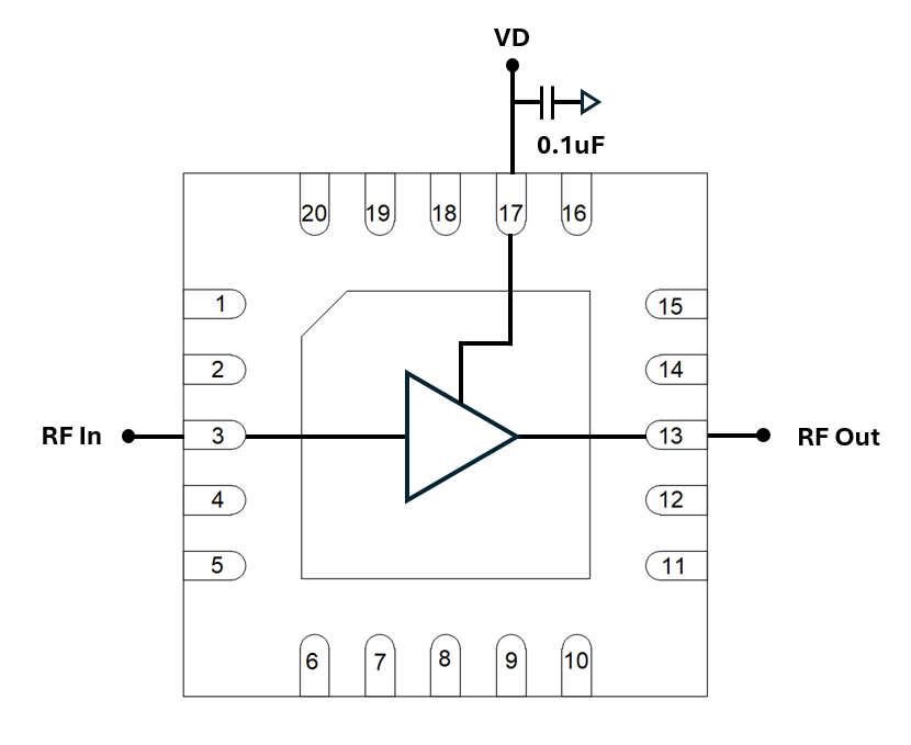
Below is the port configuration diagram for the ADM-11122PSM (X-ray view).
Sales: 408-778-9952 | General: 408-778-4200 | Fax: 408-778-4300
Sales & Customer Support: [email protected]
Tech Support: [email protected]
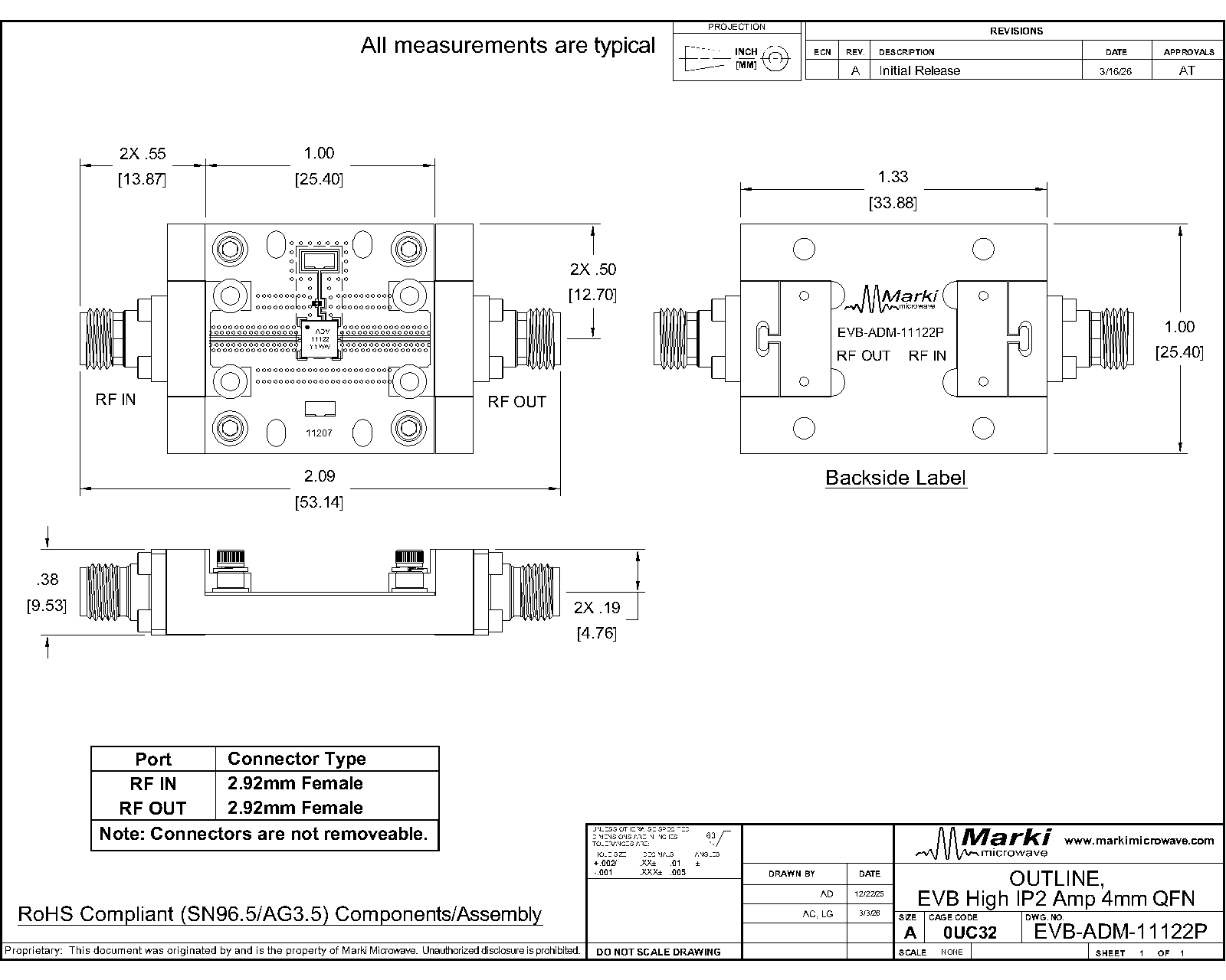
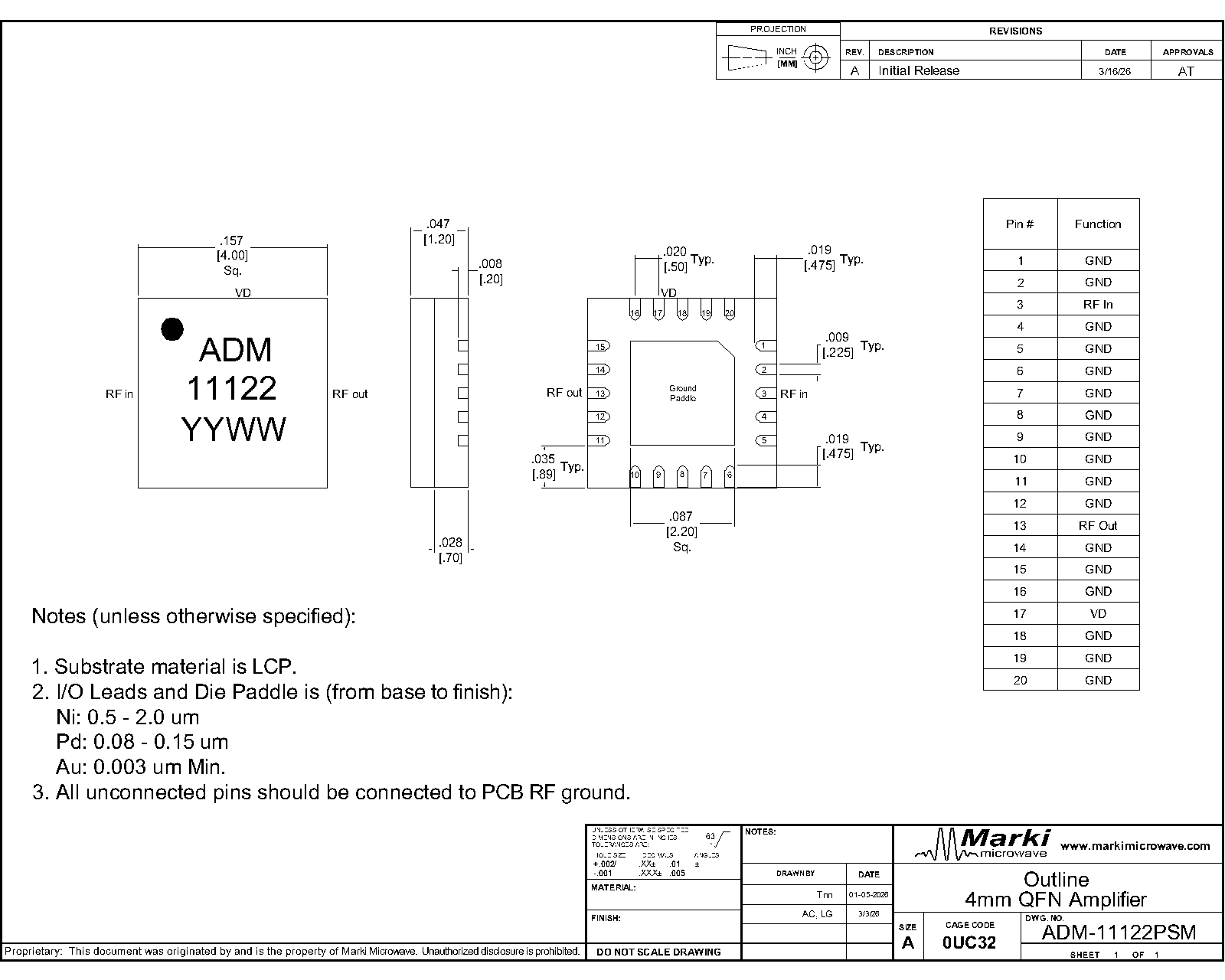
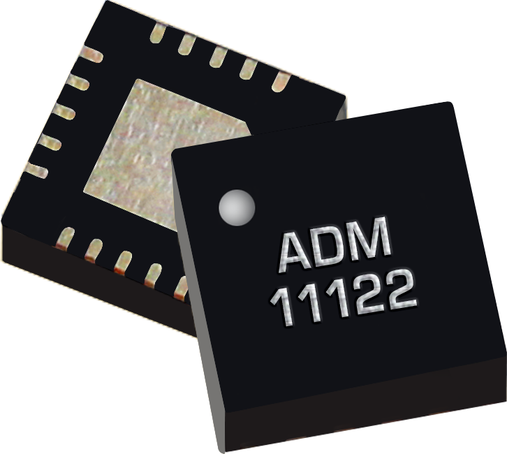
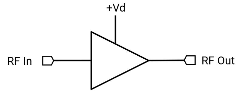
The ADM-11122PSM is a surface-mount, wideband, high output IP2, gain block amplifier designed to operate from 2 to 20 GHz. It provides 19 dB typical small-signal gain across the band, along with 4.2 dB typical noise figure and 13.7 dBm typical output P1dB. The amplifier also delivers 55 dBm typical output IP2, making it well suited for direct-conversion EW systems and other wideband signal chain applications where gain and second-order linearity are critical. The device is internally matched to 50 ohms at both input and output, and operates with a +4 V supply voltage, drawing just 84 mA. The ADM-11122PSM is packaged in a compact 4 x 4 mm plastic QFN for easy integration with automated assembly processes.
| Part Number | Description | Package | Green Status | Product Lifecycle | Export Classification |
|---|---|---|---|---|---|
| ADM-11122PSM | 2 - 20 GHz, Wideband High OIP2 Amplifier | Plastic QFN | REACH RoHS | Released | EAR99 |
| EVB-ADM-11122P | Evaluation Board, 2-20 GHz Wideband High OIP2 Amplifier | EVB | REACH RoHS | Released | EAR99 |
ADM-11122PSM
2 - 20 GHz, Wideband High OIP2 Amplifier
| Revision Code | Revision Date | Comment |
|---|---|---|
| - | 2026-03-27 | Initial Release |
ADM-11122PSM
2 - 20 GHz, Wideband High OIP2 Amplifier
Below is the port configuration diagram for the ADM-11122PSM (X-ray view).
| Port | Function | Description | DC Equivalent Circuit |
|---|---|---|---|
| Ground Paddle | Ground | Ground paddle and non-connected pins must be connected to a DC/RF ground potential with high thermal and electrical conductivity, and low inductance. |  |
| Pin 13 | RF Output | Pin 13 is the amplifier's RF output pin. This port is internally matched to 50 Ohms and is internally DC shorted to GND. This pin may be left floating if no DC is present on the line but should be DC blocked otherwise. |  |
| Pin 17 | Vd | Pin 17 is the DC bias supply for the amplifier. The voltage at this pin should be set to 4V for normal operation. This part requires an off-chip bypass capacitor of 0.1uF installed at this pin as close to the IC as possible. See applications circuit. |  |
| Pin 3 | RF Input | Pin 3 is the amplifier's RF input pin. This port is internally matched to 50 Ohms and is internally DC shorted to GND. This pin may be left floating if no DC is present on the line but should be DC blocked otherwise. | |
ADM-11122PSM
2 - 20 GHz, Wideband High OIP2 Amplifier
The Absolute Maximum Ratings indicate limits beyond which damage may occur to the device. If these limits are exceeded, the device may be inoperable or have a reduced lifetime. This amplifier is designed and characterized in a 50Ω system, and operation in a reflective environment can cause performance degradation.
| Parameter | Maximum Rating | Unit |
|---|---|---|
| Maximum Operating Temperature | 85 | °C |
| Maximum Storage Temperature | 150 | °C |
| Max Junction Temperature for MTTF > 1E6 hours | 175 | °C |
| Minimum Operating Temperature | -40 | °C |
| Minimum Storage Temperature | -65 | °C |
| Positive Drain Supply Current (with RF Input) | 134 | mA |
| Positive Drain Supply Voltage (Vd) | 6 | V |
| RF Input Power | 10 | dBm |
| Thermal Resistance, θJC | 50 | ºC/W |
| Parameter | Details | Rating |
|---|---|---|
| ESD | 250 to < 500 Volts | HBM Class 1A |
| Dimensions | - | 4 x 4 mm |
| Moisture Sensitivity Level | - | MSL 1 |
The Recommended Operating Conditions indicate the limits, inside which the device should be operated, to guarantee the performance given in Electrical Specifications. Operating outside these limits may not necessarily cause damage to the device, but the performance may degrade outside the limits of the Electrical Specifications. For limits, above which damage may occur, see Absolute Maximum Ratings .
| Parameter | Min | Nominal | Max | Unit |
|---|---|---|---|---|
| Positive DC Current (Id) (No RF Input) | 60 | 84 | 107 | mA |
| Ambient Temperature | -40 | 25 | 85 | °C |
| Power Supply DC Voltage | 3 | 4 | 5 | V |
ADM-11122PSM
2 - 20 GHz, Wideband High OIP2 Amplifier
The electrical specifications apply at TA=+25°C in a 50Ω system. QFNs are 100% RF tested.
| Parameter | Test Conditions | Minimum Frequency (GHz) | Maximum Frequency (GHz) | Min | Typ | Max | Unit |
|---|---|---|---|---|---|---|---|
| Small Signal Gain | Vd = 4V, Id = 84mA, -25dBm input power | 2 | 20 | - | 19 | - | dB |
| Input Return Loss | Vd = 4V, Id = 84mA, -25dBm input power | 2 | 20 | - | 10 | - | dB |
| Output Return Loss | Vd = 4V, Id = 84mA, -25dBm input power | 2 | 20 | - | 10 | - | dB |
| Reverse Isolation | Vd = 4V, Id = 84mA, -25dBm input power | 2 | 20 | - | 35 | - | dB |
| Noise Figure | Vd = 4V, Id = 84mA | 2 | 20 | - | 4.2 | - | dB |
| Output P1dB | Vd = 4V, Id = 84mA | 2 | 20 | - | 13.7 | - | dBm |
| Saturated Output Power | Vd = 4V, Id = 84mA | 2 | 20 | - | 14.7 | - | dBm |
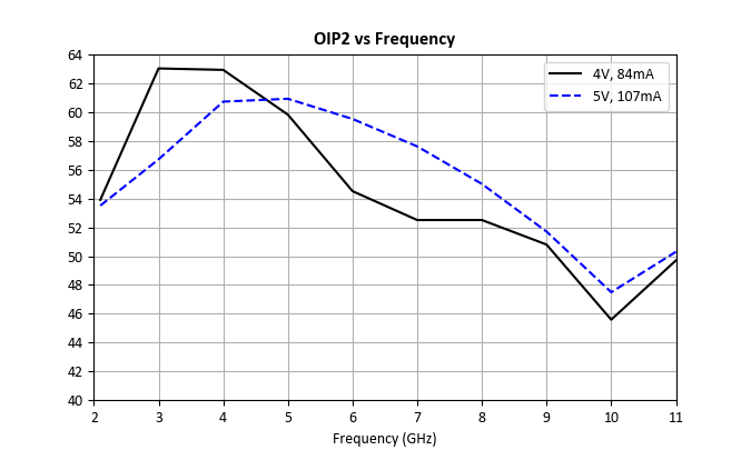
| Output IP2 | Vd = 4V, Id = 84mA, -25dBm input tone power, 1 MHz spacing | 2 | 11 | - | 55 | - | dBm |
| Output IP3 | Vd = 4V, Id = 84mA, -15dBm input tone power, 1 MHz spacing | 2 | 20 | - | 26 | - | dBm |
| Input IP3 | Vd = 4V, Id = 84mA, -15dBm input tone power, 1 MHz spacing | 2 | 20 | - | 7.6 | - | dBm |
| Current Consumption 1 | VD = 4V | - | - | - | 84 | - | mA |
| Parameter | Test Conditions | Minimum Frequency (GHz) | Maximum Frequency (GHz) | Min | Typ | Max | Unit |
|---|---|---|---|---|---|---|---|
| Small Signal Gain | Vd = 4V, Id = 84mA, -25dBm input power | 2 | 20 | - | 19 | - | dB |
| Input Return Loss | Vd = 4V, Id = 84mA, -25dBm input power | 2 | 20 | - | 10 | - | dB |
| Output Return Loss | Vd = 4V, Id = 84mA, -25dBm input power | 2 | 20 | - | 10 | - | dB |
| Reverse Isolation | Vd = 4V, Id = 84mA, -25dBm input power | 2 | 20 | - | 35 | - | dB |
| Noise Figure | Vd = 4V, Id = 84mA | 2 | 20 | - | 4.2 | - | dB |
| Output P1dB | Vd = 4V, Id = 84mA | 2 | 20 | - | 13.7 | - | dBm |
| Saturated Output Power | Vd = 4V, Id = 84mA | 2 | 20 | - | 14.7 | - | dBm |
| Output IP2 | Vd = 4V, Id = 84mA, -25dBm input tone power, 1 MHz spacing | 2 | 11 | - | 55 | - | dBm |
| Output IP3 | Vd = 4V, Id = 84mA, -15dBm input tone power, 1 MHz spacing | 2 | 20 | - | 26 | - | dBm |
| Input IP3 | Vd = 4V, Id = 84mA, -15dBm input tone power, 1 MHz spacing | 2 | 20 | - | 7.6 | - | dBm |
| Current Consumption 1 | VD = 4V | - | - | - | 84 | - | mA |
[1] Bias conditions for Id tested with no RF input power.
ADM-11122PSM
2 - 20 GHz, Wideband High OIP2 Amplifier
%20vs.%20Frequency.png)
%20vs.%20Frequency.png)
%20vs.%20Frequency.png)
%20vs.%20Frequency.png)
%20vs.%20Frequency.png)
%20vs.%20Frequency%20over%20Bias.png)
%20vs.%20Frequency.png)
ADM-11122PSM
2 - 20 GHz, Wideband High OIP2 Amplifier
%20vs.%20Frequency.png)
ADM-11122PSM
2 - 20 GHz, Wideband High OIP2 Amplifier
%20vs.%20Frequency%20over%20Temperature%20at%20Vd=4V,%20Id=84mA.png)
%20vs.%20Frequency%20over%20Temperature%20at%20Vd=5V,%20Id=107mA.png)
%20vs.%20Frequency%20over%20Temperature%20at%20Vd=4V,%20Id=84mA.png)
%20vs.%20Frequency%20over%20Temperature%20at%20Vd=5V,%20Id=107mA.png)
ADM-11122PSM
2 - 20 GHz, Wideband High OIP2 Amplifier
ADM-11122PSM
2 - 20 GHz, Wideband High OIP2 Amplifier
ADM-11122PSM
2 - 20 GHz, Wideband High OIP2 Amplifier
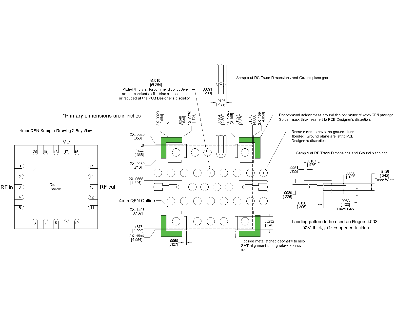
Download : Footprint Drawing
ADM-11122PSM
2 - 20 GHz, Wideband High OIP2 Amplifier