Port Diagram
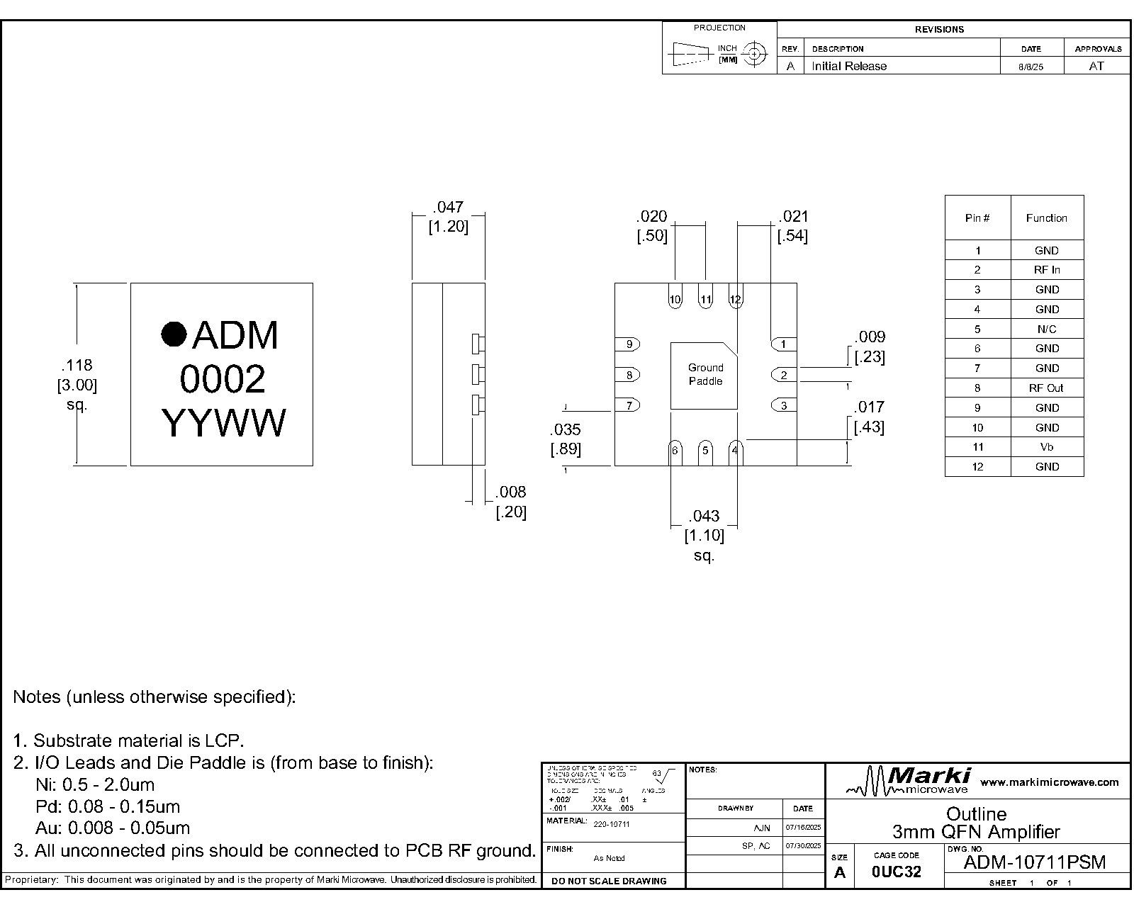
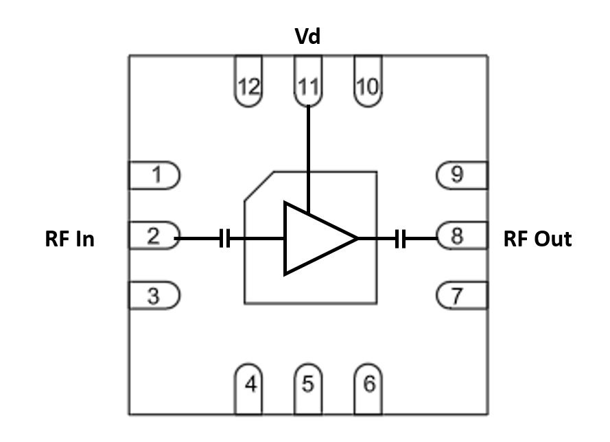
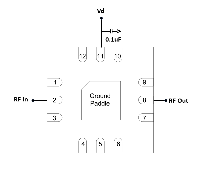
A port diagram of the ADM-10711PSM is shown below.
Sales: 408-778-9952 | General: 408-778-4200 | Fax: 408-778-4300
Sales & Customer Support: [email protected]
Tech Support: [email protected]
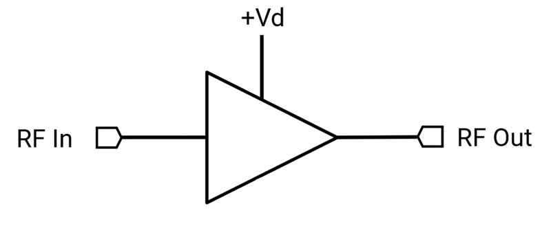
The ADM-10711PSM is a broadband low noise amplifier covering 8 to 12 GHz. Designed for ultra-low power consumption, it operates from a single 3 V supply at only 8 mA bias current while delivering 29.1 dB small-signal gain with a typical noise figure of just 1.4 dB. Packaged in a compact 3 mm QFN package, the ADM-10711PSM is ideal for front-end applications that demand high gain with minimal added noise and minimal DC power draw. Measured small-signal S-parameters are provided to support accurate system simulations.
| Part Number | Description | Package | Green Status | Product Lifecycle | Export Classification |
|---|---|---|---|---|---|
| ADM-10711PSM | 8-12 GHz Banded Low Noise Amplifier | Plastic QFN | REACH RoHS | Released | EAR99 |
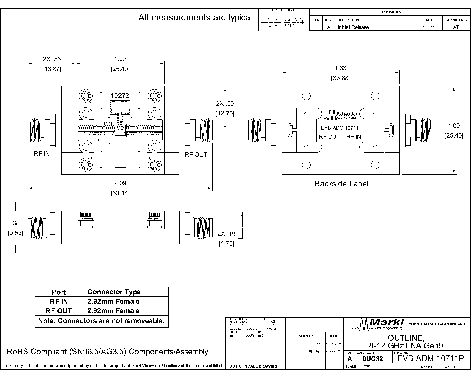
| EVB-ADM-10711P | Evaluation Board, 8-12 GHz Banded Low Noise Amplifier | EVB | REACH RoHS | Released | EAR99 |
| Part Number | Description | Package | Green Status | Product Lifecycle | Export Classification |
|---|---|---|---|---|---|
| ADM-10711PSM | 8-12 GHz Banded Low Noise Amplifier | Plastic QFN | REACH RoHS | Released | EAR99 |
| EVB-ADM-10711P | Evaluation Board, 8-12 GHz Banded Low Noise Amplifier | EVB | REACH RoHS | Released | EAR99 |
ADM-10711PSM
8-12 GHz Banded Low Noise Amplifier
| Revision Code | Revision Date | Comment |
|---|---|---|
| - | 2025-10-20 | Initial Release |
ADM-10711PSM
8-12 GHz Banded Low Noise Amplifier
A port diagram of the ADM-10711PSM is shown below.
| Port | Function | Description | DC Equivalent Circuit |
|---|---|---|---|
| GND | Ground | Ground paddle and non-connected pins must be connected to a DC/RF ground potential with high thermal and electrical conductivity, and low inductance. |  |
| Pin 11 | Vd | Pin 11 is the DC bias supply for the amplifier. The voltage at this pin should be set to 3V for normal operation. This part requires an off-chip bypass capacitor of 0.1uF installed at this pin as close to the IC as possible. See applications circuit. |  |
| Pin 1,3,4,5,6,7,9,10,12 | Ground | These pins are not internally connected to the amplifier die. It is recommended to connect these pins to ground to provide RF isolation and mechanical stability. See the recommended landing pattern for details. Datasheet performance was measured with these pins connected to GND. | - |
| Pin 2 | RF Input | Pin 2 is the amplifier's RF input pin. This port is internally matched to 50 Ohms and is internally DC blocked. |  |
| Pin 8 | RF Output | Pin 8 is the amplifier's RF output pin. This port is internally matched to 50 Ohms and is internally DC blocked. | |
ADM-10711PSM
8-12 GHz Banded Low Noise Amplifier
The Absolute Maximum Ratings indicate limits beyond which damage may occur to the device. If these limits are exceeded, the device may be inoperable or have a reduced lifetime. This amplifier is designed and characterized in a 50Ω system, and operation in a reflective environment can cause performance degradation.
| Parameter | Maximum Rating | Unit |
|---|---|---|
| Maximum Operating Temperature | 85 | °C |
| Maximum Storage Temperature 1 | 150 | °C |
| Max Junction Temperature for MTTF > 1E6 hours 2 | 175 | °C |
| Minimum Operating Temperature 3 | -40 | °C |
| Minimum Storage Temperature 4 | -65 | °C |
| Positive Drain Supply Current (with RF Input) | 19 | mA |
| Positive Drain Supply Voltage (Vd) | 6 | V |
| RF Input Power | 10 | dBm |
[1][2][3][4] TBD
| Parameter | Details | Rating |
|---|---|---|
| ESD | < 250 Volts | HBM Class 0 |
| Dimensions | - | 3 x 3 mm |
| Moisture Sensitivity Level | - | MSL 1 |
The Recommended Operating Conditions indicate the limits, inside which the device should be operated, to guarantee the performance given in Electrical Specifications. Operating outside these limits may not necessarily cause damage to the device, but the performance may degrade outside the limits of the Electrical Specifications. For limits, above which damage may occur, see Absolute Maximum Ratings .
| Parameter | Min | Nominal | Max | Unit |
|---|---|---|---|---|
| Ambient Temperature | -40 | 25 | 85 | °C |
| Power Supply DC Voltage | 3 | 3 | 6 | V |
| Positive DC Current (Id) (No RF Input) | 8 | 8 | 19 | mA |
ADM-10711PSM
8-12 GHz Banded Low Noise Amplifier
The electrical specifications apply at TA=+25°C in a 50Ω system. QFNs are 100% RF tested.
| Parameter | Test Conditions | Minimum Frequency (GHz) | Maximum Frequency (GHz) | Min | Typ | Max | Unit |
|---|---|---|---|---|---|---|---|
| Small Signal Gain | 3V bias, -30 dBm Input Power | 8 | 12 | - | 29.1 | - | dB |
| Input Return Loss | 3V bias, -30 dBm Input Power | 8 | 12 | - | 19 | - | dB |
| Output Return Loss | 3V bias, -30 dBm Input Power | 8 | 12 | - | 16 | - | dB |
| Reverse Isolation | 3V bias, -30dBm Input Power | 8 | 12 | - | 53 | - | dB |
| Noise Figure | 3V bias, -30 dBm Input Power | 8 | 12 | - | 1.4 | - | dB |
| Output P1dB | 3V bias | 8 | 12 | - | 3 | - | dBm |
| Output IP3 | 3V bias | 8 | 12 | - | 15 | - | dBm |
| Current Consumption 1 | 3V bias | - | - | - | 8 | - | mA |
[1] Bias conditions for Id tested with no RF input power. Bias conditions presented as Vd.
ADM-10711PSM
8-12 GHz Banded Low Noise Amplifier
Measurement data de-embedded using standard evaluation board and external wideband test equipment bias tees.
%20vs.%20Frequency%20over%20Bias.png)
%20vs.%20Frequency%20over%20Bias.png)
%20vs.%20Frequency%20over%20Bias.png)
%20vs.%20Frequency%20over%20Bias.png)
%20vs.%20Frequency%20over%20Bias.png)
%20vs.%20Frequency%20over%20Bias.png)
%20vs.%20Frequency%20over%20Bias.png)
ADM-10711PSM
8-12 GHz Banded Low Noise Amplifier
%20vs.%20Frequency%20over%20Temperature%20at%20Vd=3V,%20Id=8mA.png)
%20vs.%20Frequency%20over%20Temperature%20at%20Vd=4V,%20Id=12mA.png)
%20vs.%20Frequency%20over%20Temperature%20at%20Vd=3V,%20Id=8mA.png)
%20vs.%20Frequency%20over%20Temperature%20at%20Vd=4V,%20Id=12mA.png)
ADM-10711PSM
8-12 GHz Banded Low Noise Amplifier
ADM-10711PSM
8-12 GHz Banded Low Noise Amplifier
ADM-10711PSM
8-12 GHz Banded Low Noise Amplifier
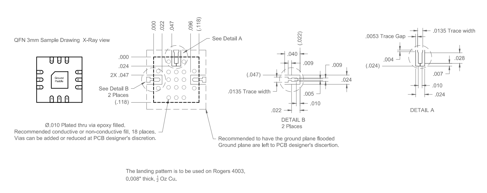
Download : Footprint Drawing
ADM-10711PSM
8-12 GHz Banded Low Noise Amplifier