Device Overview

General Description

The ADM-0026-5929SM is a broadband, efficient GaAs PHEMT distributed amplifier in a 4mm QFN surface mount package. It is designed to provide optimal LO drive for T3 mixers and offers 13 dB typical gain and 20 dBm typical saturated output power for 165 mA of current. Extended high frequency gain offers improved harmonic generation and rise times improving T3 linearity. The ADM-0026-5929SM is biased with a 5-7 volt positive bias and an optional current reducing negative voltage with external bias tee. The ADM-0026-5929SM is an excellent alternative to competing GaAs PHEMT distributed amplifiers.

Photo of ADM-0026-5929SM

Features

  • Fast <10 ps risetime
  • 3rd and 5th Harmonic Generation
  • Broadband 50 Ω Matching
  • Unconditionally Stable

Applications

  • Amplification Clock Signals
  • Electronic Warfare
  • Test and Measurement Equipment

Functional Block Diagram

Block Diagram

Part Ordering Options

Part NumberDescriptionPackagePacking SizeGreen StatusProduct LifecycleExport Classification
ADM-0026-5929SMBroadband Distributed AmplifierQFN-

REACH

RoHS

ReleasedEAR99
EVAL-ADM-5929SMEvaluation Board, Broadband Distributed 26.5 GHz Amplifier EVAL-

REACH

RoHS

ReleasedEAR99
ADM-0026-5929TRTape and Reel, Broadband Distributed AmplifierQFN7"

REACH

RoHS

ReleasedEAR99

Table Of Contents

Revision History

Revision CodeRevision DateComment
-2015-01-01Datasheet Initial Release
A2019-10-01Plating call-out is now ENEPIG effective starting on D/C 1846

Rev: A | Copyright © 2015, 2019 Marki Microwave LLC.

2

Port Configuration and Functions

Rev: A | Copyright © 2015, 2019 Marki Microwave LLC.

3

Port Functions

PortFunctionDescriptionDC Equivalent
Circuit
11Vg Gate control for the amplifier. External decoupling resistor/capacitor is required.Equivalent circuit for the Vg
1-3, 5-10, 12-15, 17-20, 22, 24NC These pins are not connected internally. Datasheet performance is tested with NC pins grounded.-
16RF Out / Vd This pad is DC coupled and matched to 50 Ω.Equivalent circuit for the RF Out / Vd
21Vd2 External decoupling resistor/capacitor is required.Equivalent circuit for the Vd2
4RF Input This pin is DC coupled and matched to 50 Ω.Equivalent circuit for the RF Input
PaddleGnd Ground pad should be connected to RF/DC ground with low electrical and thermal resistance.-

Rev: A | Copyright © 2015, 2019 Marki Microwave LLC.

4

Specifications

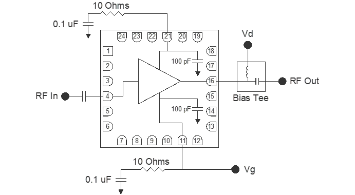
Absolute Maximum Ratings

ParameterMaximum RatingUnit
Maximum Operating Temperature 85°C
Maximum Storage Temperature 150°C
Minimum Operating Temperature -55°C
Minimum Storage Temperature -65°C
Negative Bias Current 2mA
Negative Bias Voltage -2V
Positive Bias Current 275mA
Positive Bias Voltage 9V
Power Dissipation 2W
RF Input Power 20dBm
Thermal Resistance 0.873ºC/W

Package Information

ParameterDetailsRating
ESD< 250 VoltsHBM Class 0
Dimensions-4 x 4 mm
Moisture Sensitivity Level-MSL 1

Rev: A | Copyright © 2015, 2019 Marki Microwave LLC.

5

Electrical Specifications

Specifications measured in a 50-Ohm system.

ParameterTest ConditionsMinimum
Frequency
(GHz)
Maximum
Frequency
(GHz)
MinTypMaxUnit
Current Consumption Vd: +5.0 to +7.0
Vg: -0.25 Volts
0 26.5-165-mA
Current Consumption Vd: +5.0 to +7.0
Vg: 0 Volts
0 26.5-225-mA
Input Power for Saturation -0 26.551012dBm
Noise Figure -0 26.5-5.5-dB
Output IP3 -0 26.5-26-dBm
Output P1dB -0 26.5-15-dBm
Return Loss -0 26.5-14-dB
Saturated Output Power With Negative Bias
0 26.5-20-dBm
Small Signal Gain With Negative Bias
0 26.5-13-dB

Rev: A | Copyright © 2015, 2019 Marki Microwave LLC.

6

Typical Performance Plots - Positive Only (+3 to +7V) Bias (Pin 16 Output), Grounded Gate (Pin 11)

Small Signal Gain (dB) graph for ADM-0026-5929SM
Saturated Output Power (dBm) graph for ADM-0026-5929SM
Reverse Isolation (dB) graph for ADM-0026-5929SM
Small Signal Return Loss graph for ADM-0026-5929SM
Input IP3 (dBm) graph for ADM-0026-5929SM
Output IP3 (dBm) graph for ADM-0026-5929SM
Even Harmonic Generation (dBm) +10 dBm Input graph for ADM-0026-5929SM
Odd Harmonic Generation (dBm) +10 dBm Input graph for ADM-0026-5929SM

Rev: A | Copyright © 2015, 2019 Marki Microwave LLC.

7

Output P1dB (dBm) graph for ADM-0026-5929SM
Band 1 Group Delay (ps) graph for ADM-0026-5929SM
Noise Figure (dB) graph for ADM-0026-5929SM
Current Consumption (mA) with 10 GHz Input graph for ADM-0026-5929SM

Rev: A | Copyright © 2015, 2019 Marki Microwave LLC.

8

Typical Performance Plots - +5 to +7V Positive Bias (Pin 16 Output), -.25 Negative Bias (Pin11)

Small Signal Gain (dB) graph for ADM-0026-5929SM
Small Signal Gain (dB) over Temperature graph for ADM-0026-5929SM
Saturated Output Power (dBm) graph for ADM-0026-5929SM
Reverse Isolation (dB) graph for ADM-0026-5929SM
Input Small Signal Return Loss (dB) graph for ADM-0026-5929SM
Input Small Signal Return Loss (dB) over Temperature graph for ADM-0026-5929SM
Output Small Signal Return Loss (dB) graph for ADM-0026-5929SM
Output P1dB (dBm) graph for ADM-0026-5929SM

Rev: A | Copyright © 2015, 2019 Marki Microwave LLC.

9

Output Small Signal Return Loss (dB) over Temperature graph for ADM-0026-5929SM
Input IP3 (dBm) graph for ADM-0026-5929SM
Output IP3 (dBm) graph for ADM-0026-5929SM
Even Harmonic Generation (dBm) +10 dBm Input graph for ADM-0026-5929SM
Odd Harmonic Generation (dBm) +10 dBm Input graph for ADM-0026-5929SM
Band 1 Group Delay (ps) graph for ADM-0026-5929SM
Noise Figure (dB) graph for ADM-0026-5929SM
Current Consumption (mA) with 10 GHz Input graph for ADM-0026-5929SM

Rev: A | Copyright © 2015, 2019 Marki Microwave LLC.

10

Application Circuit

Application Circuit for ADM-0026-5929SM

Rev: A | Copyright © 2015, 2019 Marki Microwave LLC.

11

Mechanical Data

Rev: A | Copyright © 2015, 2019 Marki Microwave LLC.

12

Rev: A | Copyright © 2015, 2019 Marki Microwave LLC.

13

Evaluation Board - Outline Drawing

Outline Drawing

Rev: A | Copyright © 2015, 2019 Marki Microwave LLC.

14