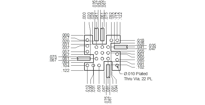
Port Diagram
Sales: 408-778-9952 | General: 408-778-4200 | Fax: 408-778-4300
Sales & Customer Support: [email protected]
Tech Support: [email protected]
The ADM-0012-5931SM is a small, low power, and economical T3 driver or T3A pre-amplifier. It is a GaAs PHEMT distributed amplifier in a 3mm QFN surface mount package. The ADM-0012-5931SM can provide LO drive for ‘L’, ‘M’, ‘I’, and ‘H’ level mixers, with 11.5 dB typical gain and +19 dBm typical saturated output power for only 85 mA of current. The amplifier can be biased with internal circuitry, or with an external bias network for lower voltage and single supply operation.


| Part Number | Description | Package | Packing Size | Green Status | Product Lifecycle | Export Classification |
|---|---|---|---|---|---|---|
| ADM-0012-5931SM | Broadband Distributed Amplifier | QFN | - | REACH RoHS | Released | EAR99 |
| EVAL3-ADM-5931 | Evaluation Board, Broadband Distributed Amplifier | EVAL | - | REACH RoHS | Released | EAR99 |
| ADM-0012-5931TR | Tape and Reel, Broadband Distributed Amplifier | QFN | 7" | REACH RoHS | Released | EAR99 |
ADM-0012-5931SM
Broadband Distributed Amplifier
| Revision Code | Revision Date | Comment |
|---|---|---|
| - | 2015-01-01 | Datasheet Initial Release |
| A | 2019-07-01 | Changed thermal resistance to TBD |
| B | 2020-12-01 | Added Max Junction Temp Specification |
ADM-0012-5931SM
Broadband Distributed Amplifier
ADM-0012-5931SM
Broadband Distributed Amplifier
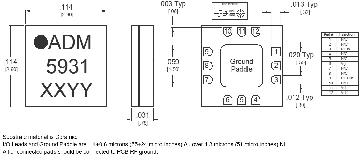
| Port | Function | Description | DC Equivalent Circuit |
|---|---|---|---|
| 11 | Vd | Power supply voltage for the amplifier. External decoupling resistor/capacitor is required. |  |
| 12 | Vd2 | This pin is left open for Internal Vd Bias. This pin is connected to Pin 11 (Vd) for external bias (pin 16 with bias tee). | - |
| 1, 2, 4, 5, 7, 8,10 | NC | These pins are not connected internally. Datasheet performance is tested with NC pins grounded. | - |
| 3 | RF Input | This pin is DC coupled and matched to 50 Ω. |  |
| 6 | Vg | Gate control for the amplifier. External decoupling resistor/capacitor is required. |  |
| 9 | RF Output | This pad is DC coupled and matched to 50 Ω. |  |
| Paddle | Gnd | Ground pad should be connected to RF/DC ground with low electrical and thermal resistance. |  |
ADM-0012-5931SM
Broadband Distributed Amplifier
| Parameter | Maximum Rating | Unit |
|---|---|---|
| Maximum Operating Temperature | 85 | °C |
| Maximum Storage Temperature | 150 | °C |
| Max Junction Temperature to Maintain 10⁶ Hours Mean Time to Failure (MTTF): | 175 | °C |
| Minimum Operating Temperature | -55 | °C |
| Minimum Storage Temperature | -65 | °C |
| Negative Bias Current | 2 | mA |
| Negative Bias Voltage | -2 | V |
| Positive Bias Bias Voltage – Internal Bias Tee | 13 | V |
| Positive Bias Current | 150 | mA |
| Positive Bias Voltage – External Bias Tee | 9 | V |
| Power Dissipation | 875 | mW |
| RF Input Power | 15 | dBm |
| Parameter | Details | Rating |
|---|---|---|
| ESD | < 250 Volts | HBM Class 0 |
| Dimensions | - | 3 x 3 mm |
| Moisture Sensitivity Level | - | MSL 1 |
ADM-0012-5931SM
Broadband Distributed Amplifier
Specifications measured in a 50-Ohm system.
| Parameter | Test Conditions | Minimum Frequency (GHz) | Maximum Frequency (GHz) | Min | Typ | Max | Unit |
|---|---|---|---|---|---|---|---|
| Current Consumption | Vd: +10.0 to +12.0 (Internal) Vg:-0.25 Volts | 0 | 12 | - | 85 | - | mA |
| Current Consumption | Vd: +5.0 to +7.0 (External) Vg: -0.25 Volts | 0 | 12 | - | 85 | - | mA |
| Current Consumption | Vd: +5.0 to +7.0 (External) Vg: 0 Volts | 0 | 12 | - | 115 | - | mA |
| Input Power for Saturation | - | 0 | 12 | 5 | 10 | 12 | dBm |
| Input Return Loss | - | 0 | 12 | - | 13 | - | dB |
| Noise Figure | - | 0 | 12 | - | 4.5 | - | dB |
| Output IP3 | - | 0 | 12 | - | 26 | - | dBm |
| Output P1dB | - | 0 | 12 | - | 16 | - | dBm |
| Output Return Loss | - | 0 | 12 | - | 14 | - | dB |
| Saturated Output Power | With Negative Bias | 0 | 12 | - | 19 | - | dBm |
| Small Signal Gain | With Negative Bias | 0 | 12 | - | 11.5 | - | dB |
ADM-0012-5931SM
Broadband Distributed Amplifier


ADM-0012-5931SM
Broadband Distributed Amplifier


ADM-0012-5931SM
Broadband Distributed Amplifier
.png)
ADM-0012-5931SM
Broadband Distributed Amplifier


ADM-0012-5931SM
Broadband Distributed Amplifier


ADM-0012-5931SM
Broadband Distributed Amplifier


ADM-0012-5931SM
Broadband Distributed Amplifier


ADM-0012-5931SM
Broadband Distributed Amplifier
ADM-0012-5931SM
Broadband Distributed Amplifier
Download : Footprint Drawing