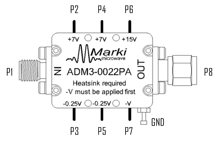
Port Diagram
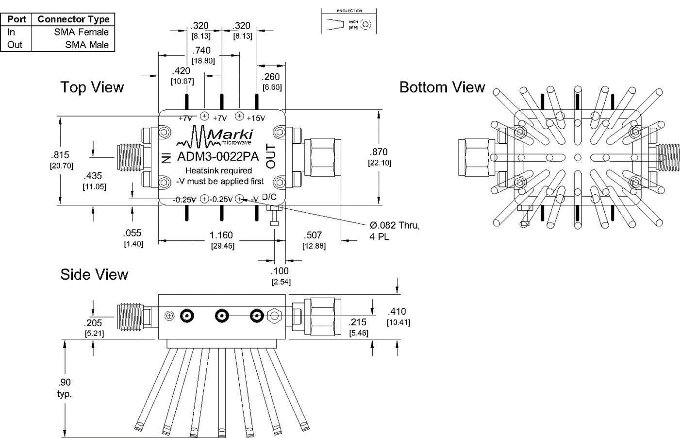
A top-down view of the ADM3-0022PA package outline drawing is shown below.
Sales: 408-778-9952 | General: 408-778-4200 | Fax: 408-778-4300
Sales & Customer Support: [email protected]
Tech Support: [email protected]
The ADM3-0022PA has the gain and output power to produce 1W of output power from a +0 dBm input power up to 22 GHz. It contains 3 broadband amplifier stages in series in a single package with built-in equalization to provide a flat gain and output power curve. This product is an unprotected amplifier module intended for lab use. See notes section for handling and operating precautions.

| Part Number | Description | Package | Connectors | Green Status | Product Lifecycle | Export Classification |
|---|---|---|---|---|---|---|
| ADM3-0022PA | Broadband Power Amplifier | PA | Standard | REACH RoHS | Released | EAR99 |
| ADM3-0022PA-H | Broadband Power Amplifier | PA-H | Standard | REACH RoHS | Released | EAR99 |
ADM3-0022PA-H
Broadband Power Amplifier
| Revision Code | Revision Date | Comment |
|---|---|---|
| - | 2019-08-01 | Datasheet Initial Release |
| A | 2020-01-01 | Format Update |
ADM3-0022PA-H
Broadband Power Amplifier
A top-down view of the ADM3-0022PA package outline drawing is shown below.
ADM3-0022PA-H
Broadband Power Amplifier
| Port | Function | Connector Type | Description | DC Equivalent Circuit |
|---|---|---|---|---|
| GND | Gnd | - | Must be connected to a DC/RF ground potential with high thermal and electrical conductivity. Ensure that the ground voltage is a common reference potential to all DC power supplies |  |
| Port 1 | RF Input | SMAF | Port 1 is the RF input of the amplifier. It is DC blocked and has a 50 Ω input impedance. |  |
| Port 2 | Vd1 | - | Port 2 is the positive DC voltage supply pin for the 1st amplifier stage. Nominally 3V – 7V, 155 mA |  |
| Port 3 | Vg1 | - | Port 3 is the negative DC voltage bias pin for the 1st amplifier stage. Nominally -0.25V, <1 mA |  |
| Port 4 | Vd2 | - | Port 4 is the positive DC voltage supply pin for the 2nd amplifier stage. Nominally 3V – 7V, 155 mA | |
| Port 5 | Vg2 | - | Port 5 is the negative DC voltage bias pin for the 2nd amplifier stage. Nominally -0.25V, <1 mA | |
| Port 6 | Vd3 | - | Port 6 is the positive DC voltage supply pin for the 3rd amplifier stage. Nominally 13V-15V, 450 mA. Vg3 must be applied to Port 7 prior to application of Vd3! | |
| Port 7 | Vg3 | - | Port 7 is the negative DC voltage bias pin for the 3rd amplifier stage. Nominally -0.85V, <1 mA. Must be applied prior to application of Vd3 on Port 6! | |
| Port 8 | RF Output | SMAM | Port 8 is the RF output of the amplifier. It is DC blocked and has a 50 Ω output impedance. Load must be applied to meet maximum VSWR spec. | |
ADM3-0022PA-H
Broadband Power Amplifier
The Absolute Maximum Ratings indicate limits beyond which damage may occur to the device. If these limits are exceeded, the device may be inoperable or have a reduced lifetime.
| Parameter | Maximum Rating | Unit |
|---|---|---|
| Maximum Ambient Air Temperature (with PA-H Package) | 40 | °C |
| Maximum Case Temperature 1 | 60 | °C |
| Maximum Storage Temperature | 125 | °C |
| Minimum Ambient Air Temperature (with PA-H Package) | -40 | °C |
| Minimum Case Temperature 2 | -40 | °C |
| Minimum Storage Temperature | -65 | °C |
| Negative Bias Voltage 1 (Port 3) | -2 | V |
| Negative Bias Voltage 2 (Port 5) | -2 | V |
| Negative Bias Voltage 3 (Port 7) | -3 | V |
| Output Load VSWR | 7 | - |
| Positive Bias Current 1 (Port 2) | 275 | mA |
| Positive Bias Current 2 (Port 4) | 275 | mA |
| Positive Bias Current 3 (Port 6) | 500 | mA |
| Positive Bias Voltage 1 (Port 2) | 9 | V |
| Positive Bias Voltage 2 (Port 4) | 9 | V |
| Positive Bias Voltage 3 (Port 6) | 15 | V |
| RF Input Power (Port 1) | 5 | dBm |
[1] Air flow across heat sink required to maintain case temperature below limits
[2] Air flow across heat sink required to maintain case temperature below limits.
| Parameter | Details | Rating |
|---|---|---|
| ESD | 250 to < 500 Volts | HBM Class 1A |
| Weight | Package name: PA-H | 44.5g |
| Dimensions | - | 29.46 x 22.10 mm |
The Recommended Operating Conditions indicate the limits, inside which the device should be operated, to guarantee the performance given in Electrical Specifications. Operating outside these limits may not necessarily cause damage to the device, but the performance may degrade outside the limits of the electrical specifications. For limits, above which damage may occur, see Absolute Maximum Ratings. To keep the temperature below 60°C, the user is advised to use a fan to keep a constant airflow over the heat sink.
| Parameter | Min | Nominal | Max | Unit |
|---|---|---|---|---|
| Ambient Temperature | -40 | 25 | 40 | °C |
| Positive DC Voltage (Port 2, Port 4) | 3 | 7 | 7 | V |
| Positive DC Current (Port 2, Port 4) | 100 | 155 | 275 | mA |
| Positive DC Voltage (Port 6) | 12 | 15 | 15 | V |
| Positive DC Current (Port 6) 1 | 200 | 450 | 500 | mA |
[1] To protect the output stage of the module, ensure that Port 6 never pulls more than 500 mA of DC current. Current pull will increase with increased RF input power and with decreased negative bias on Port 7.
ADM3-0022PA-H
Broadband Power Amplifier
The electrical specifications apply at TA=+25°C in a 50Ω system. Min and Max limits apply only to our connectorized units and are guaranteed at TA=+25°C.
| Parameter | Test Conditions | Minimum Frequency (GHz) | Maximum Frequency (GHz) | Min | Typ | Max | Unit |
|---|---|---|---|---|---|---|---|
| Current Consumption | 15V/-0.85 (Ports 6/7), no RF | - | - | - | 185 | - | mA |
| Current Consumption | 7V/-0.25V (Ports 2/3), no RF | - | - | - | 155 | - | mA |
| Current Consumption | 7V/-0.25V (Ports 4/5), no RF | - | - | - | 155 | - | mA |
| Input IP3 | 7V/-0.25V, 7V/-0.25V, 15V/-0.85V, -25 dBm Input Power | - | - | - | -4 | - | dBm |
| Input Return Loss | 7V/-0.25V, 7V/-0.25V, 15V/-0.85V, -25 dBm Input Power | - | - | - | 14 | - | dB |
| Noise Figure | 7V/-0.25V, 7V/-0.25V, 15V/-0.85V, -25 dBm Input Power | - | - | - | 5 | - | dB |
| Output IP3 | 7V/-0.25V, 7V/-0.25V, 15V/-0.85V, -25 dBm Input Power | - | - | - | 31 | - | dBm |
| Output P1dB | 7V/-0.25V, 7V/-0.25V, 15V/-0.85V | - | - | - | 26 | - | dBm |
| Output Return Loss | 7V/-0.25V, 7V/-0.25V, 15V/-0.85V, -25 dBm Input Power | - | - | - | 14 | - | dB |
| Reverse Isolation | 7V/-0.25V, 7V/-0.25V, 15V/-0.85V, -25 dBm Input Power | - | - | - | 70 | - | dB |
| Saturated Output Power | 7V/-0.25V, 7V/-0.25V, 15V/-0.85V, -5 dBm Input Power | - | - | 25 | 30 | - | dBm |
| Small Signal Gain | 7V/-0.25V, 7V/-0.25V, 15V/-0.85V, -25 dBm Input Power | - | - | 28 | 35 | - | dB |
ADM3-0022PA-H
Broadband Power Amplifier


ADM3-0022PA-H
Broadband Power Amplifier


ADM3-0022PA-H
Broadband Power Amplifier