Port Diagram
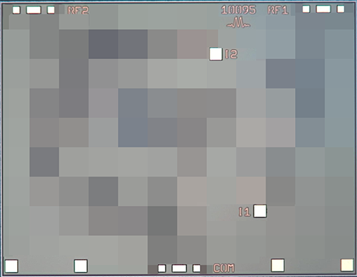
A top-down view of the MSW2-00002CH die is show below.

Sales: 408-778-9952 | General: 408-778-4200 | Fax: 408-778-4300
Sales & Customer Support: [email protected]
Tech Support: [email protected]
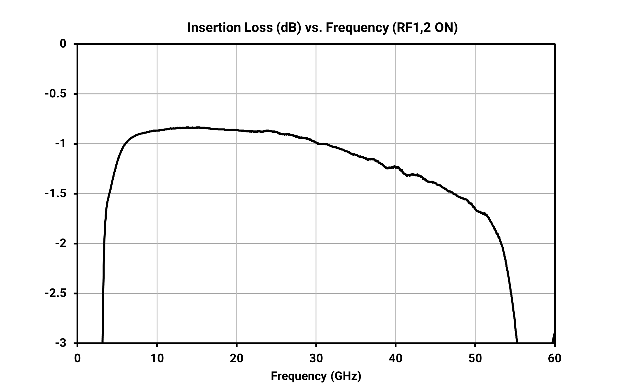
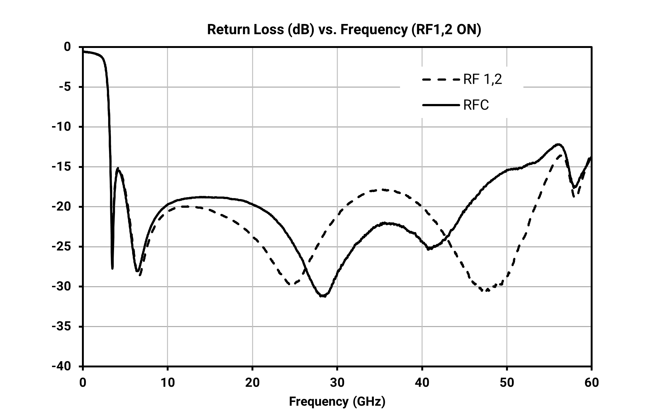
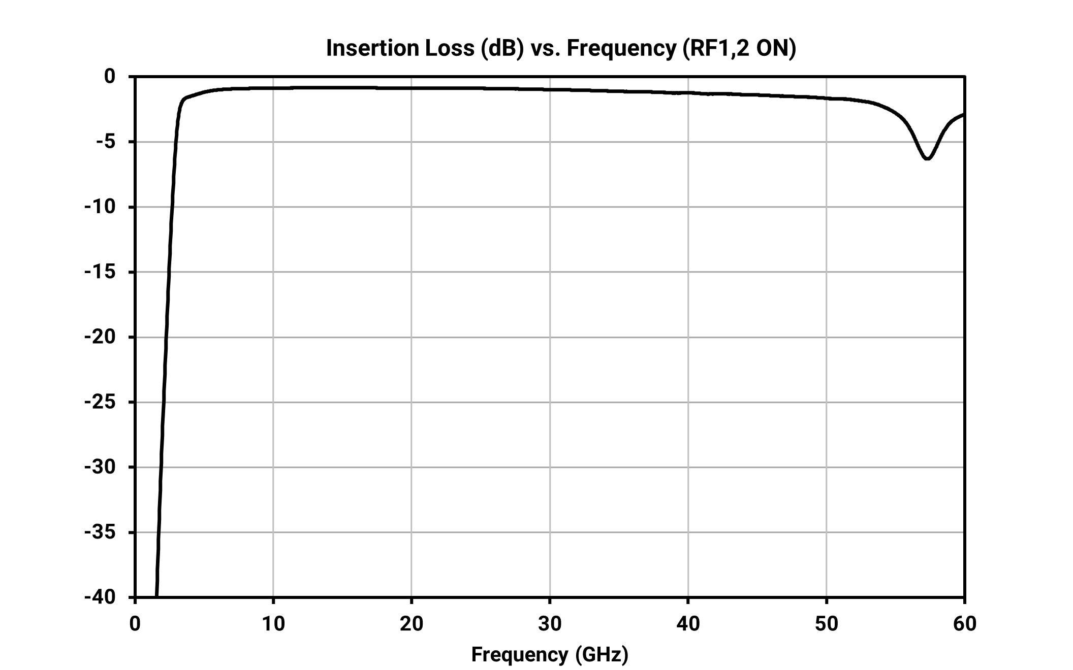
The MSW2-00002CH is a reflective, single-pole double throw (SPDT) switch. The switch operates from 4 GHz to 50 GHz with average insertion loss and isolation of 1.0 dB and 48 dB respectively. The MSW2-00002CH requires positive and negative 5V supply inputs to control switch states. This switch has a 50-Ohm characteristic impedance. The MSW2-00002CH is available as a wire-bondable die.

| Part Number | Description | Package | Green Status | Product Lifecycle | Export Classification |
|---|---|---|---|---|---|
| MSW2-00002CH | 4-50 GHz MMIC GaAs PIN SPDT Switch | CH | REACH RoHS | Released | EAR99 |
| Part Number | Description | Package | Green Status | Product Lifecycle | Export Classification |
|---|---|---|---|---|---|
| MSW2-00002CH | 4-50 GHz MMIC GaAs PIN SPDT Switch | CH | REACH RoHS | Released | EAR99 |
MSW2-00002CH
4-50 GHz MMIC GaAs PIN SPDT Switch
| Revision Code | Revision Date | Comment |
|---|---|---|
| - | 2025-05-23 | Initial Release |
| A | 2025-06-02 | Updated IP3 and P1dB plots frequency range. |
MSW2-00002CH
4-50 GHz MMIC GaAs PIN SPDT Switch
A top-down view of the MSW2-00002CH die is show below.
MSW2-00002CH
4-50 GHz MMIC GaAs PIN SPDT Switch
| Port | Function | Description | DC Equivalent Circuit |
|---|---|---|---|
| GND | Ground | DC and RF ground is provided through the backside of the die. The die should be connected to a DC/RF ground with high thermal and electrical conductivity. | - |
| I1 | VCTRL1 | I1 is the control input pad for port RF1. Control voltages applied to this pad and the I2 pad will result in the active switch path being turned ON or OFF as described in the Application Information section of the datasheet. Nominal positive and negative control voltage for this port are +5V and -5V respectively. The bias circuit attached to this pad should be capable of sourcing or sinking at least 10mA of DC control current. | - |
| I2 | VCTRL2 | I2 is the control input pad for port RF2. Control voltages applied to this pad and the I1 pad will result in the active switch path being turned ON or OFF as described in the Application Information section of the datasheet. Nominal positive and negative control voltage for this port are +5V and -5V respectively. The bias circuit attached to this pad should be capable of sourcing or sinking at least 10mA of DC control current. | - |
| RF1 | Input/Output 1 | RF port 1 of the device, impedance looking into this port matches RFC load impedance in the ON state. This port is reflective and shorted to GND in the OFF state. This port is internally DC shorted to GND and should have an external DC block installed if DC exists on the RF1 line. | - |
| RF2 | Input/Output 2 | RF port 2 of the device, impedance looking into this port matches RFC load impedance in the ON state. This port is reflective and shorted to GND in the OFF state. This port is internally DC shorted to GND and should have an external DC block installed if DC exists on the RF2 line. | - |
| RFC | Common | RF common port of the device. The input impedance of this port is determined by the RF output port terminations. Output ports should be connected to a 50 Ohm load for normal operation. This port is internally DC shorted to GND and should have an external DC block installed if DC exists on the RFC line. | - |
MSW2-00002CH
4-50 GHz MMIC GaAs PIN SPDT Switch
The Absolute Maximum Ratings indicate limits beyond which damage may occur to the device. If these limits are exceeded, the device may become inoperable or have a reduced lifetime.
| Parameter | Maximum Rating | Unit |
|---|---|---|
| Max DC on any RF port 1 | 0 | V |
| Maximum Operating Temperature | 100 | °C |
| Maximum Storage Temperature | 125 | °C |
| Minimum Operating Temperature | -55 | °C |
| Minimum Storage Temperature | -65 | °C |
| Negative Supply Voltage | -10 | V |
| Positive Supply Voltage | 10 | V |
[1] RF ports are internally shorted to GND and should not have DC voltage applied.
| Parameter | Details | Rating |
|---|---|---|
| Dimensions | - | 3.10 x 2.40 mm |
The Recommended Operating Conditions indicate the limits, inside which the device should be operated, to guarantee the performance given in Electrical Specifications. Operating outside these limits may not necessarily cause damage to the device, but the performance may degrade outside the limits of the electrical specifications. For limits, above which damage may occur, see Absolute Maximum Ratings.
| Parameter | Min | Nominal | Max | Unit |
|---|---|---|---|---|
| Control Voltage Low, VINL | -8 | -5 | -3 | V |
| Ta Ambient Temperature | -55 | 25 | 100 | °C |
| Control Current, IINL | -5 | -10 | -15 | mA |
| Control Voltage High, VINH | 3 | 5 | 8 | V |
| Control Current, IINH | 5 | 10 | 15 | mA |
MSW2-00002CH
4-50 GHz MMIC GaAs PIN SPDT Switch
The electrical specifications apply at TA=+25 °C in a 50 Ω system. Unless otherwise noted, all specifications are for I1=±10mA, I2=±10mA and V1 and V2 = ±5V (both switch paths) with all ports terminated into 50 Ω loads.
| Parameter | Test Conditions | Minimum Frequency (GHz) | Maximum Frequency (GHz) | Min | Typ | Max | Unit |
|---|---|---|---|---|---|---|---|
| Insertion Loss | I1=±10mA, I2=±10mA, V1 and V2=±5V | 4 | 50 | - | 1 | - | dB |
| Return Loss | I1=±10mA, I2=±10mA, V1 and V2=±5V | 4 | 50 | - | 22 | - | dB |
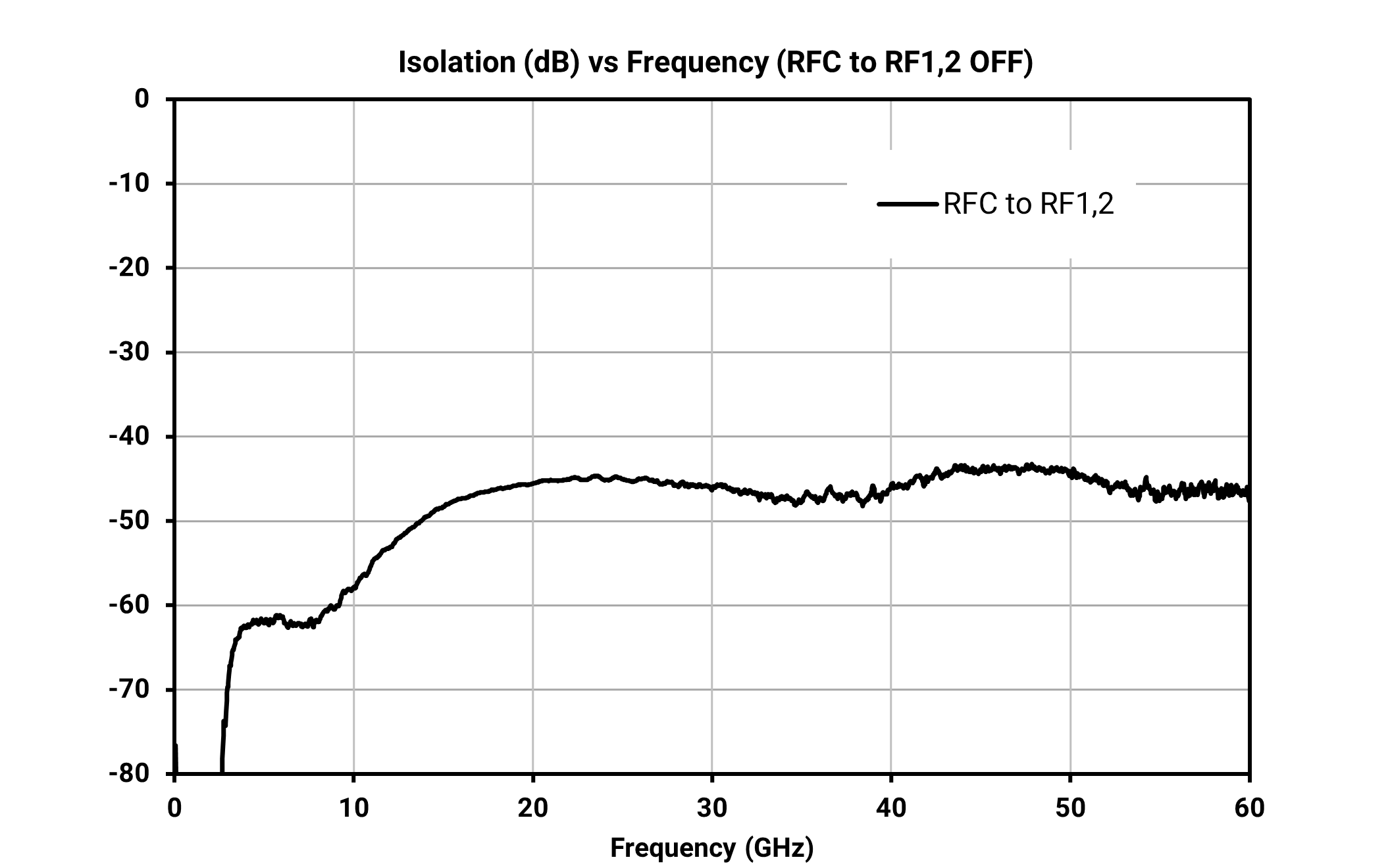
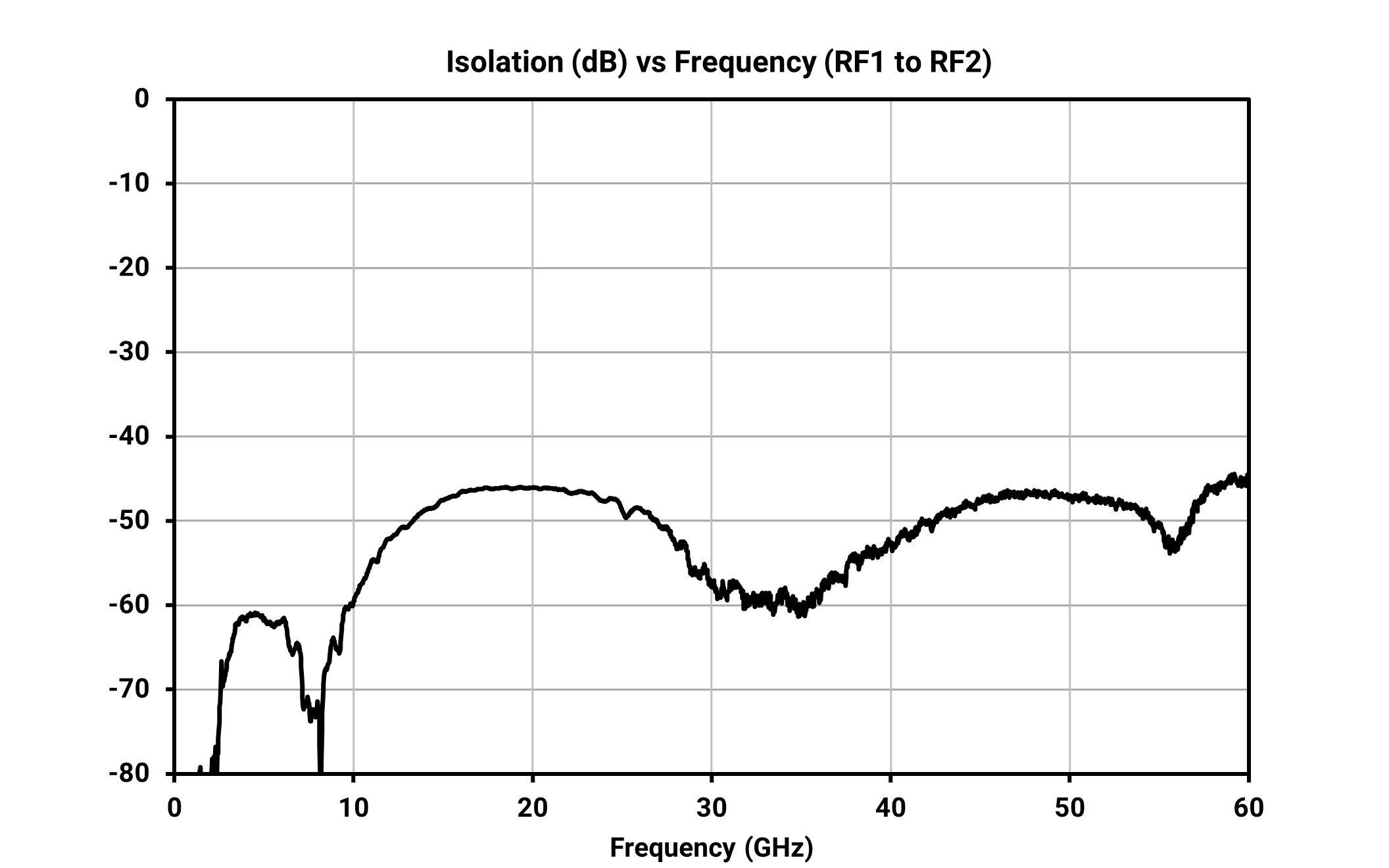
| Isolation | I1=±10mA, I2=±10mA, V1 and V2=±5V | 4 | 50 | - | 53 | - | dB |
| Isolation, RFC to any non-active Port | I1=±10mA, I2=±10mA, V1 and V2=±5V | 4 | 50 | - | 48 | - | dB |
| Input P1dB | I1=±10mA, I2=±10mA, V1 and V2=±5V | 4 | 18 | - | 26 | - | dBm |
| Input IP3 | Two Tones @ +12dBm, dF=1 MHz, I1=±10mA, I2=±10mA, V1 and V2=±5V | 2 | 20 | - | 41 | - | dBm |
| RF Settling Time | 50% V1 and V2 to 0.1dB final RF output | 4 | 50 | - | 19 | - | ns |
| Risetime/Falltime | 10-90% of RF output | 4 | 50 | - | 4 | - | ns |
| On-Time | 50% V1 and V2 to 90% RF output | 4 | 50 | - | 17 | - | ns |
| Nominal RF Impedance | I1=±10mA, I2=±10mA, V1 and V2=±5V | - | - | - | 50 | - | Ω |
| Parameter | Test Conditions | Minimum Frequency (GHz) | Maximum Frequency (GHz) | Min | Typ | Max | Unit |
|---|---|---|---|---|---|---|---|
| Insertion Loss | I1=±10mA, I2=±10mA, V1 and V2=±5V | 4 | 50 | - | 1 | - | dB |
| Return Loss | I1=±10mA, I2=±10mA, V1 and V2=±5V | 4 | 50 | - | 22 | - | dB |
| Isolation | I1=±10mA, I2=±10mA, V1 and V2=±5V | 4 | 50 | - | 53 | - | dB |
| Isolation, RFC to any non-active Port | I1=±10mA, I2=±10mA, V1 and V2=±5V | 4 | 50 | - | 48 | - | dB |
| Input P1dB | I1=±10mA, I2=±10mA, V1 and V2=±5V | 4 | 18 | - | 26 | - | dBm |
| Input IP3 | Two Tones @ +12dBm, dF=1 MHz, I1=±10mA, I2=±10mA, V1 and V2=±5V | 2 | 20 | - | 41 | - | dBm |
| RF Settling Time | 50% V1 and V2 to 0.1dB final RF output | 4 | 50 | - | 19 | - | ns |
| Risetime/Falltime | 10-90% of RF output | 4 | 50 | - | 4 | - | ns |
| On-Time | 50% V1 and V2 to 90% RF output | 4 | 50 | - | 17 | - | ns |
| Nominal RF Impedance | I1=±10mA, I2=±10mA, V1 and V2=±5V | - | - | - | 50 | - | Ω |
MSW2-00002CH
4-50 GHz MMIC GaAs PIN SPDT Switch
Unless otherwise noted, plotted data is for I1=±10mA, I2=±10mA and V1 and V2 = ±5V (both switch paths) with all ports terminated into 50 Ω loads.

MSW2-00002CH
4-50 GHz MMIC GaAs PIN SPDT Switch

MSW2-00002CH
4-50 GHz MMIC GaAs PIN SPDT Switch

MSW2-00002CH
4-50 GHz MMIC GaAs PIN SPDT Switch
Download : Outline 2D Drawing
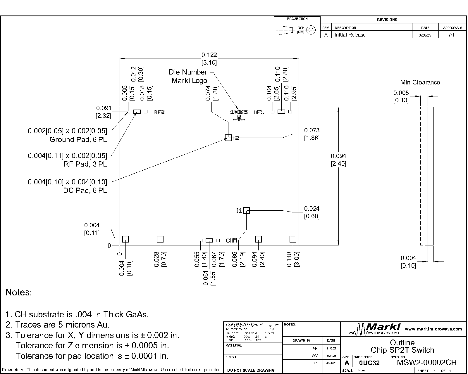
1. CH substrate is .004 in Thick GaAs.
2. Traces are 5 microns Au.
3. Tolerance for X, Y dimensions is ± 0.002 in.
Tolerance for Z dimension is ± 0.0005 in.
Tolerance for pad location is ± 0.0001 in.