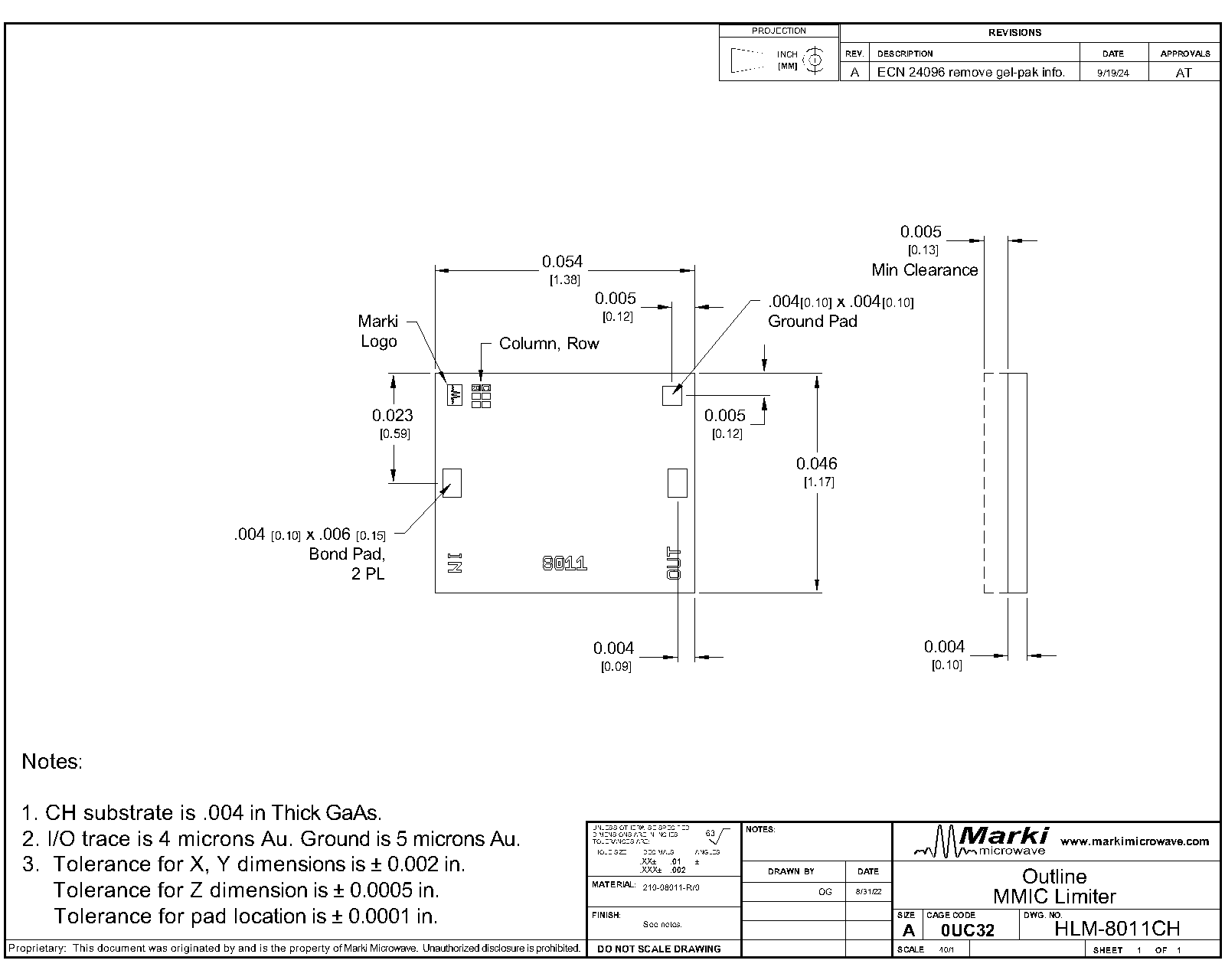
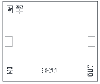
Port Diagram
A top-down view of the HLM-8011’s CH package outline drawing is shown below. The HLM-8011 has the input and output ports given in Port Functions.
Sales: 408-778-9952 | General: 408-778-4200 | Fax: 408-778-4300
Sales & Customer Support: [email protected]
Tech Support: [email protected]
The HLM-8011 is a high-power GaAs Schottky diode signal limiter featuring high IP3 and high power handling. It offers low insertion loss and low return loss from DC through Ka band and has a typical 1dB compression point of +9dBm. Its low flat leakage makes it ideal for protecting sensitive components and for applications requiring high linearity. It is available as a wire bondable die and as a connectorized module.

N/A

HLM-8011CH
Low Flat Leakage DC-30GHz Limiter
| Revision Code | Revision Date | Comment |
|---|---|---|
| - | 2023-03-01 | Initial Release |
| A | 2025-03-19 | Updated Catalog Outline | ECN 24096 |
| B | 2026-06-02 | Added Recovery Time and Spike Leakage |
HLM-8011CH
Low Flat Leakage DC-30GHz Limiter
A top-down view of the HLM-8011’s CH package outline drawing is shown below. The HLM-8011 has the input and output ports given in Port Functions.
| Port | Function | Description | DC Equivalent Circuit |
|---|---|---|---|
| GND | Ground | CH package ground path is provided through the substrate and ground bond pads. |  |
| IN | Input | The input port is diode connected for the CH package. |  |
| OUT | Output | The output port is diode connected for the CH package. | |
HLM-8011CH
Low Flat Leakage DC-30GHz Limiter
The Absolute Maximum Ratings indicate limits beyond which damage may occur to the device. If these limits are exceeded, the device may be inoperable or have a reduced lifetime.
| Parameter | Maximum Rating | Unit |
|---|---|---|
| Average Power Handling at Input Port 1 | 30 | dBm |
| Maximum Operating Temperature | 100 | °C |
| Maximum Storage Temperature | 125 | °C |
| Minimum Operating Temperature | -55 | °C |
| Minimum Storage Temperature | -65 | °C |
| Peak Power Handling at Input Port 2 | 4.5 | W |
| RF Power Handling , Average | 1 | W |
| RF Power Handling , Peak | 4.5 | W |
[1] See Input Power at Observed Failure for basis of average power handling specs. 33.5dBm at 2GHz derated linearly to 30dBm at 30GHz.
[2] See Input Power at Observed Failure for basis of peak power handling specs. 6.5W at 2GHz derated linearly to 4.5W at 18GHz.
| Parameter | Details | Rating |
|---|---|---|
| ESD | 250 to < 500 Volts | HBM Class 1A |
| Dimensions | - | 1.38x1.17 mm |
HLM-8011CH
Low Flat Leakage DC-30GHz Limiter
The electrical specifications apply at TA=+25°C in a 50Ω system. Typical data shown is for the connectorized U-package limiter unless otherwise specified. Linear Specifications valid for input power up to the 0.1dB compression point. See typical performance plots for P0.1dB graph. Min and Max limits are guaranteed at TA=+25°C.
| Parameter | Test Conditions | Minimum Frequency (GHz) | Maximum Frequency (GHz) | Min | Typ | Max | Unit |
|---|---|---|---|---|---|---|---|
| Spike Leakage | - | - | - | - | 0.1 | - | erg |
| Recovery Time | - | - | - | - | 8 | - | ns |
| Flat Leakage at 1W | DC – 30GHz | 0 | 30 | - | 7 | - | dBm |
| Input P1dB | DC – 30GHz | 0 | 30 | - | 10 | - | dBm |
| Insertion Loss | DC – 30GHz | 0 | 30 | - | 0.4 | 1.5 | dB |
| Return Loss | DC – 30GHz | 0 | 30 | - | 23 | - | dB |
| Flat Leakage | - | - | - | - | 7 | - | dBm |
| Flat Leakage | - | - | - | - | 7 | - | dBm |
| Input P1dB | - | - | - | - | 10 | - | dBm |
| Input P1dB | - | - | - | - | 10 | - | dBm |
HLM-8011CH
Low Flat Leakage DC-30GHz Limiter


HLM-8011CH
Low Flat Leakage DC-30GHz Limiter


HLM-8011CH
Low Flat Leakage DC-30GHz Limiter


HLM-8011CH
Low Flat Leakage DC-30GHz Limiter
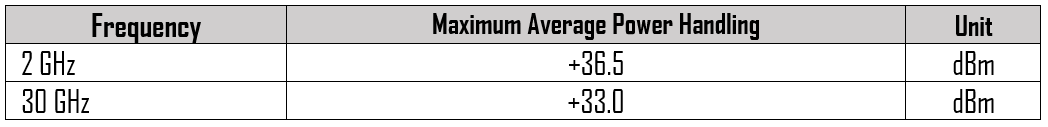
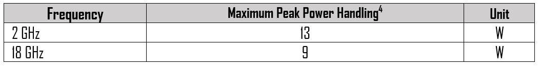
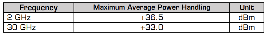
Power handling specification is based on tests performed at different combinations of room temperature and frequency. Input power was increased until catastrophic failure was observed. Results are shown in the following table. The power handling specification listed in Absolute Maximum Ratings is based on the worst observed power handling derated by 3dB.
HLM-8011CH
Low Flat Leakage DC-30GHz Limiter
Performance plots for the connectorized module are shown for measurements where directly probed measurements of the die are unavailable. Note that the following measurements include losses from connectors and microstrip traces.


HLM-8011CH
Low Flat Leakage DC-30GHz Limiter


HLM-8011CH
Low Flat Leakage DC-30GHz Limiter


HLM-8011CH
Low Flat Leakage DC-30GHz Limiter
Power handling specification is based on tests performed at different combinations of room temperature and frequency. Input power was increased until catastrophic failure was observed. Results are shown in the following table. The power handling specification listed in the Absolute Maximum Ratings section is based on the worst observed power handling derated by 3dB.
Performance plots for the connectorized module are shown for measurements where directly probed measurements of the die are unavailable. Note that the following measurements include losses from connectors and microstrip traces.

HLM-8011CH
Low Flat Leakage DC-30GHz Limiter