Port Diagram
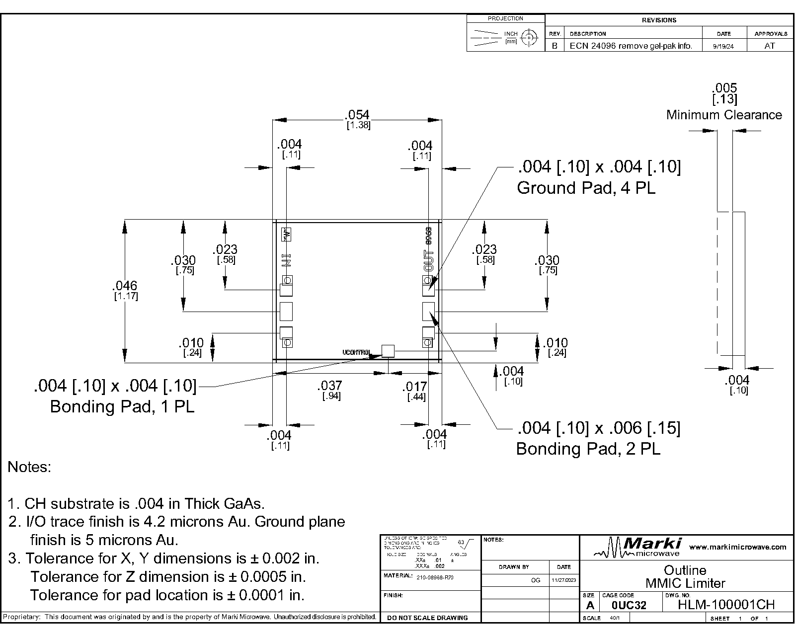
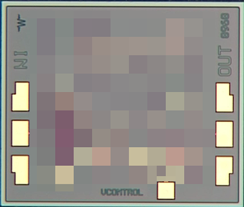
A top-down view of the HLM-100001CH's package outline drawing is shown below. The HLM-100001CH has the input and output ports given in Port Functions.

Sales: 408-778-9952 | General: 408-778-4200 | Fax: 408-778-4300
Sales & Customer Support: [email protected]
Tech Support: [email protected]
The HLM-100001CH is a high-power GaAs Schottky diode signal limiter featuring high IP3 over a broad DC-10GHz bandwidth. It offers low insertion loss and excellent return loss from DC through X band and has a typical 1 dB compression point of 11 dBm. Its high power handling makes it ideal for protecting sensitive components and for applications requiring high linearity. It is available as a wire-bondable die.

| Part Number | Description | Package | Green Status | Product Lifecycle | Export Classification |
|---|---|---|---|---|---|
| HLM-100001CH | High Power DC - 10GHz Limiter | CH | REACH RoHS | Released | EAR99 |
| Part Number | Description | Package | Green Status | Product Lifecycle | Export Classification |
|---|---|---|---|---|---|
| HLM-100001CH | High Power DC - 10GHz Limiter | CH | REACH RoHS | Released | EAR99 |
HLM-100001CH
High Power DC - 10GHz Limiter
| Revision Code | Revision Date | Comment |
|---|---|---|
| - | 2024-03-28 | Datasheet Initial Release |
| A | 2026-06-02 | Added Recovery Time and Spike Leakage |
HLM-100001CH
High Power DC - 10GHz Limiter
A top-down view of the HLM-100001CH's package outline drawing is shown below. The HLM-100001CH has the input and output ports given in Port Functions.
| Port | Function | Description | DC Equivalent Circuit |
|---|---|---|---|
| Ground Paddle | Ground | CH package ground path is provided through the substrate and ground bond pads. |  |
| IN | Input | IN is the RF input port and is diode connected for the CH package. |  |
| OUT | Output | OUT is the RF output port and is diode connected for the CH package. | |
| VCONTROL | V Control | A 10Ω resistor with at least a 30 mA current rating must be used in series with VCONTROL and tied to ground for normal operation. |  |
HLM-100001CH
High Power DC - 10GHz Limiter
The Absolute Maximum Ratings indicate limits beyond which damage may occur to the device. If these limits are exceeded, the device may be inoperable or have a reduced lifetime.
| Parameter | Maximum Rating | Unit |
|---|---|---|
| Maximum Operating Temperature | 100 | °C |
| Maximum Storage Temperature | 125 | °C |
| Minimum Operating Temperature | -55 | °C |
| Minimum Storage Temperature | -65 | °C |
| RF Power Handling, CW @ 10 GHz, 25°C | 10 | W |
| θJC, Junction to Case Thermal Resistance | 35 | ºC/W |
RF Power Handling represents an instantaneous, catastrophic limit and it isn’t derated for frequency, temperature, pulse conditions, or unit to unit variation.
| Parameter | Details | Rating |
|---|---|---|
| Dimensions | - | 1.17 x 1.38 mm |
HLM-100001CH
High Power DC - 10GHz Limiter
The electrical specifications apply at TA=+25°C in a 50Ω system. Typical data shown is for the CH package limiter unless otherwise specified. Linear Specifications valid for input power up to the 0.1dB compression point. See typical performance plots EVB PSM Package for P0.1dB graph. Min and Max limits are guaranteed at TA=+25°C.
| Parameter | Test Conditions | Minimum Frequency (GHz) | Maximum Frequency (GHz) | Min | Typ | Max | Unit |
|---|---|---|---|---|---|---|---|
| Spike Leakage | - | - | - | - | 0.1 | - | erg |
| Recovery Time | - | - | - | - | 8 | - | ns |
| Flat Leakage 1 | - | 2 | 2 | - | 11.5 | - | dBm |
| Flat Leakage 2 | - | 10 | 10 | - | 8.5 | - | dBm |
| Input IP3 3 | DC - 10 GHz | 0 | 10 | - | 27 | - | dBm |
| Input P1dB 4 | DC - 10 GHz | 0 | 10 | - | 11 | - | dBm |
| Insertion Loss | DC - 10 GHz | 0 | 10 | - | 0.8 | 1.5 | dB |
| Return Loss | DC - 10 GHz | 0 | 10 | - | 22 | - | dB |
[1][2][3][4] Data taken from HLM-100001PSM EVB package.
HLM-100001CH
High Power DC - 10GHz Limiter


HLM-100001CH
High Power DC - 10GHz Limiter


HLM-100001CH
High Power DC - 10GHz Limiter


HLM-100001CH
High Power DC - 10GHz Limiter

HLM-100001CH
High Power DC - 10GHz Limiter