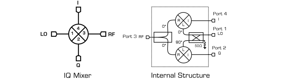
Port Diagram
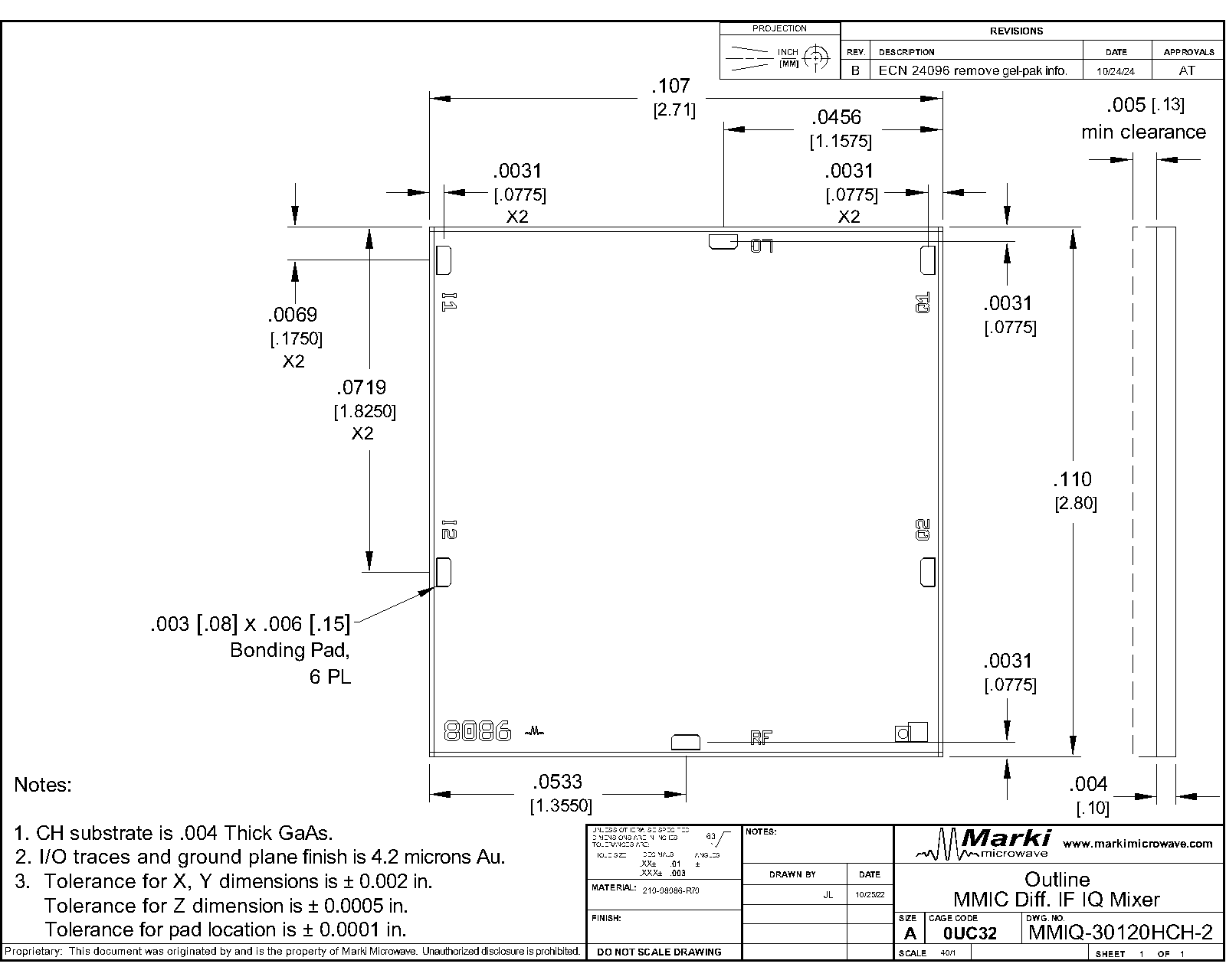
A top-down view of the MMIQ-30120H’s CH-2 package outline drawing is shown below. The mixer may be operated as either a downconverter or an upconverter. Use of the RF or I/Q as the input or output port will depend on the application.

Sales: 408-778-9952 | General: 408-778-4200 | Fax: 408-778-4300
Sales & Customer Support: [email protected]
Tech Support: [email protected]
The MMIQ-30120H is a high linearity, passive GaAs MMIC IQ mixer. This is an ultra-broadband mixer spanning 30 to 120 GHz on the RF and LO ports with an IF from DC to 30 GHz. With a typical image rejection of 27dBc from the V through W band, this mixer is an ideal candidate for mmWave I/Q frequency conversion. Both wire bondable die and connectorized modules are available.
RF/LO Frequency Range:
30 - 120 GHz
IF Frequency Range:
DC - 30 GHz
I+Q Conversion Loss: 8.5 dB
Image Rejection: 27 dBc

| Part Number | Description | Package | Connectors | Green Status | Product Lifecycle | Export Classification |
|---|---|---|---|---|---|---|
| MMIQ-30120HM | GaAs MMIC mmWave Differential IF IQ Mixer | M | Standard | REACH RoHS | Released | EAR99 |
| MMIQ-30120HCH-2 | GaAs MMIC mmWave Differential IF IQ Mixer | CH | - | REACH RoHS | Released | EAR99 |
MMIQ-30120HCH-2
GaAs MMIC mmWave Differential IF IQ Mixer
| Revision Code | Revision Date | Comment |
|---|---|---|
| - | 2023-01-01 | Datasheet Pre-Release |
MMIQ-30120HCH-2
GaAs MMIC mmWave Differential IF IQ Mixer
A top-down view of the MMIQ-30120H’s CH-2 package outline drawing is shown below. The mixer may be operated as either a downconverter or an upconverter. Use of the RF or I/Q as the input or output port will depend on the application.
MMIQ-30120HCH-2
GaAs MMIC mmWave Differential IF IQ Mixer
| Port | Function | Description | DC Equivalent Circuit |
|---|---|---|---|
| GND | Ground | CH package ground path is taken through the substrate. |  |
| Port 1 / RF | RF Input / Output | Port 1 is DC open for the CH and M packages. |  |
| Port 2 / Q2 | Q Input / Output | Port 2 is DC open for the CH and M packages | |
| Port 3 / Q1 | Q+ Input/Output | Port 3 is DC open for the CH and M packages. | |
| Port 4 / LO | LO Input/Output | Port 4 is DC open for the CH and M packages. | |
| Port 5 / I1 | I+ Input/Output | Port 5 is DC open for the CH and M packages. | |
| Port 6 / I2 | I- Input/Output | Port 6 is DC open for the CH and M packages. | |
MMIQ-30120HCH-2
GaAs MMIC mmWave Differential IF IQ Mixer
The Absolute Maximum Ratings indicate limits beyond which damage may occur to the device. If these limits are exceeded, the device may be inoperable or have a reduced lifetime.
| Parameter | Maximum Rating | Unit |
|---|---|---|
| Maximum Operating Temperature | 100 | °C |
| Maximum Storage Temperature | 125 | °C |
| Minimum Operating Temperature | -55 | °C |
| Minimum Storage Temperature | -65 | °C |
| Power Handling, at any Port | 25 | dBm |
| Parameter | Details | Rating |
|---|---|---|
| ESD | 250 to < 500 Volts | HBM Class 1A |
| Dimensions | - | 2.71 x 2.80 mm |
The Recommended Operating Conditions indicate the limits, inside which the device should be operated, to guarantee the performance given in Electrical Specifications. Operating outside these limits may not necessarily cause damage to the device, but the performance may degrade outside the limits of the electrical specifications. For limits, above which damage may occur, see Absolute Maximum Ratings.
| Parameter | Min | Nominal | Max | Unit |
|---|---|---|---|---|
| Ambient Temperature | -55 | 25 | 100 | °C |
| LO Input Power | 14 | 17 | 21 | dBm |
MMIQ-30120HCH-2
GaAs MMIC mmWave Differential IF IQ Mixer
The electrical specifications apply at TA=+25°C in a 50Ω system. Typical data shown is for a down conversion application with a sine wave LO input. Min and Max limits apply only to our connectorized units and are guaranteed at TA=+25°C
| Parameter | Test Conditions | Minimum Frequency (GHz) | Maximum Frequency (GHz) | Min | Typ | Max | Unit |
|---|---|---|---|---|---|---|---|
| Conversion Loss | RF/LO = 30 – 120 GHz I+Q = 0.1 GHz | 30 | 120 | - | 8.5 | - | dB |
| IF Frequency Range | - | - | - | 0 | - | 30 | GHz |
| Image Rejection 1 | RF/LO = 30 - 120 GHz I+Q = 0.1 GHz | 30 | 120 | - | 27 | - | dBc |
| I/Q Amplitude Balance | RF/LO = 30 - 120 GHz I+Q = 0.1 GHz | 30 | 120 | - | 1.9 | - | dB |
| LO Frequency Range | - | - | - | 30 | - | 120 | GHz |
| LO-RF Isolation | RF/LO = 30 - 120 GHz I+Q = 0.1 GHz | 30 | 120 | - | 40 | - | dB |
| Phase Balance | RF/LO = 30 - 120 GHz I+Q = 0.1 GHz | 30 | 120 | - | 2.7 | - | ° |
| RF Frequency Range | - | - | - | 30 | - | 120 | GHz |
[1] Image Rejection and Single sideband performance plots are defined by the upper sideband (USB) or lower sideband (LSB) with respect to the LO signal. Plots are defined by which sideband is selected by the external IF quadrature hybrid.
MMIQ-30120HCH-2
GaAs MMIC mmWave Differential IF IQ Mixer
Unless stated otherwise, all measurements were conducted with a single I1/I2 and a single Q1/Q2. Differential IFs were not recombined through a balun.


MMIQ-30120HCH-2
GaAs MMIC mmWave Differential IF IQ Mixer


MMIQ-30120HCH-2
GaAs MMIC mmWave Differential IF IQ Mixer


MMIQ-30120HCH-2
GaAs MMIC mmWave Differential IF IQ Mixer
Unless stated otherwise, all measurements were conducted with a single I1/I2 and a single Q1/Q2. Differential IFs were not recombined through a balun.
Performance plots for the connectorized module are shown for measurements where directly probed measurements of the die are unavailable. Note that the following measurements include losses from connectors and microstrip traces.


MMIQ-30120HCH-2
GaAs MMIC mmWave Differential IF IQ Mixer


MMIQ-30120HCH-2
GaAs MMIC mmWave Differential IF IQ Mixer

MMIQ-30120HCH-2
GaAs MMIC mmWave Differential IF IQ Mixer
MMIQ-30120HCH-2
GaAs MMIC mmWave Differential IF IQ Mixer