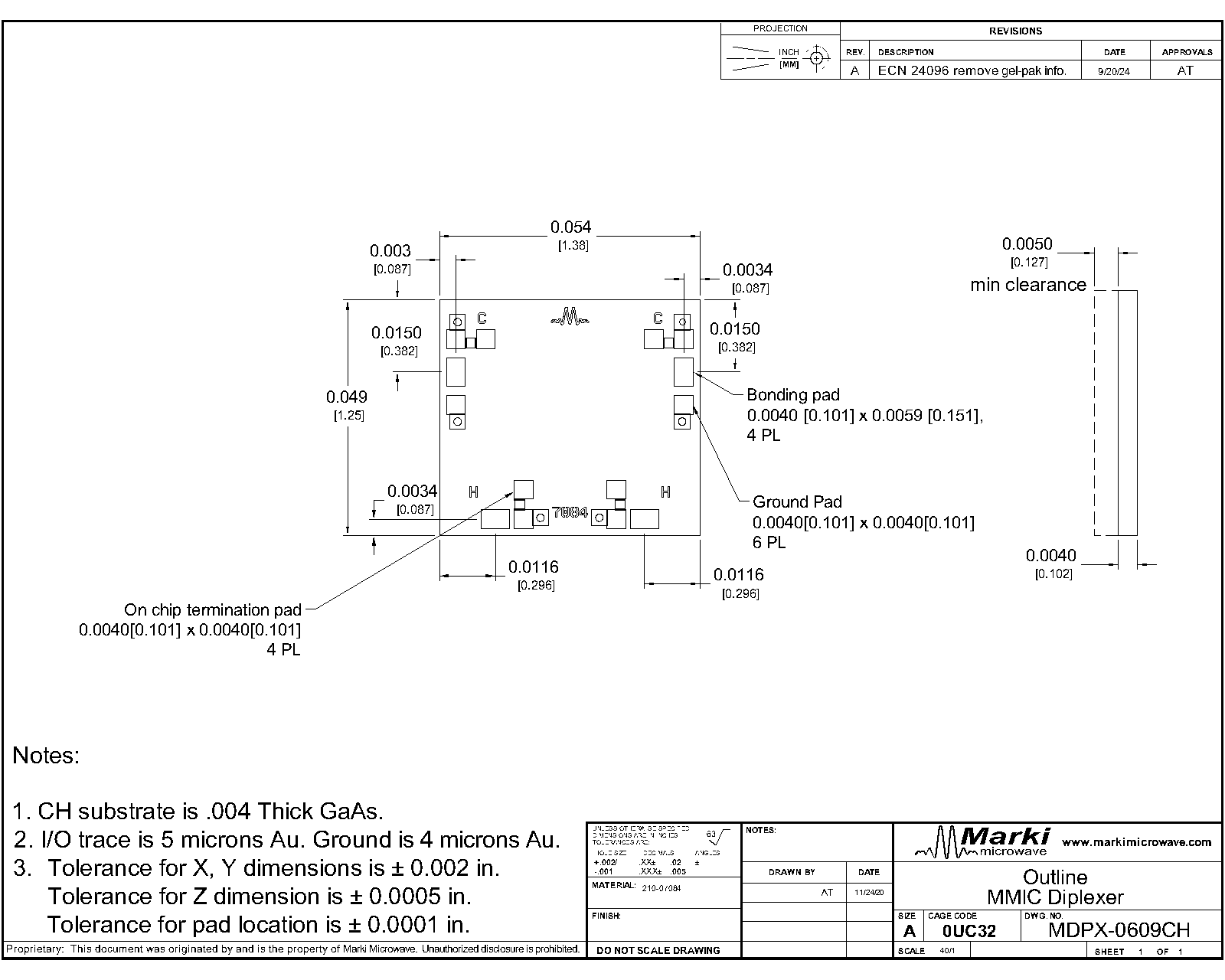
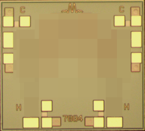
Device Overview

General Description

The MDPX-0609 is a broadband passive MMIC diplexer, a combination high pass and loss pass filter, capable of multiplexing low frequency DC to 6 GHz and high frequency 9 to 26.5 GHz signals. It can also be used as a reflectionless high pass or low pass filter when terminated with an internal/external 50 Ohm load. Passive GaAs MMIC technology allows production of smaller filter constructions that replace larger form factor circuit board constructions. Tight fabrication tolerances allow for less unit-to-unit variation than traditional filter technologies. The MDPX-0609 is available as a connectorized module and as wire bondable die. Low unit to unit variation allows for accurate simulations using the provided S3P file taken from measured production units.

Photo of MDPX-0609CH

Features

  • 8 GHz Crossover Point
  • Low <1dB typical Insertion Loss in Pass band
  • High Stop Band Suppression
  • Reflectionless Filter
  • RoHS Compliant

Applications

N/A

Functional Block Diagram

Block Diagram

Part Ordering Options

Part NumberDescriptionPackageConnectorsGreen StatusProduct LifecycleExport Classification
MDPX-0609Passive MMIC DC-6 GHz Diplexer/Reflectionless FilterUBStandard

REACH

RoHS

ReleasedEAR99
MDPX-0609CHPassive MMIC 9 - 26.5 GHz Diplexer/Reflectionless FilterCH-

REACH

RoHS

ReleasedEAR99

Table Of Contents

Revision History

Revision CodeRevision DateComment
-2021-07-01Datasheet initial Release
A2022-03-01CH Wire Bondable Die Added

Rev: A | Copyright © 2021 - 2022 Marki Microwave LLC.

2

Port Configuration and Functions

Port Diagram

The MDPX-0609CH can be used as a Diplexer, reflectionless LPF, or reflectionless HPF depending on the configuration of each port which can be seen below in the Configuration Array. For configuration A, input to the diplexer is port 1, port 2 will be the output after passing through the HPF, port 3 will be terminated with port 3R, port 4 will be the output after passing through the LPF.

Diagram of the port configuration for MDPX-0609CH

Port Functions

Configuration A

PortFunctionDescriptionDC Equivalent
Circuit
GNDGround CH package ground path is provided through the substrate and ground bond pads.Equivalent circuit for the Ground
Pad 1Input/common Pad 1 is DC short to Pad 4 and open to the other two pads and ground.Equivalent circuit for the Input/common
Pad 2RF High Band Pad 2 is DC short to ground and open to all other pads. Equivalent circuit for the RF High Band
Pad 3Terminated Pad 3 is DC short to ground and open to all other pads.Equivalent circuit for the Terminated
Pad 4RF Low Band Pad 4 is DC short to Pad 1 and open to the other two pads and ground. Equivalent circuit for the RF Low Band

Rev: A | Copyright © 2021 - 2022 Marki Microwave LLC.

3

Configuration B

PortFunctionDescriptionDC Equivalent
Circuit
GNDGround CH package ground path is provided through the substrate and ground bond pads.Equivalent circuit for the Ground
Pad 1RF Low Band Pad 1 is DC short to Pad 4 and open to the other two pads and ground. Equivalent circuit for the RF Low Band
Pad 2Terminated Pad 2 is DC short to ground and open to all other pads. Equivalent circuit for the Terminated
Pad 3RF High Band Pad 3 is DC short to ground and open to all other pads.Equivalent circuit for the RF High Band
Pad 4Input/common Pad 4 is DC short to Pad 1 and open to the other two pads and ground. Equivalent circuit for the Input/common

Rev: A | Copyright © 2021 - 2022 Marki Microwave LLC.

4

Configuration C

PortFunctionDescriptionDC Equivalent
Circuit
GNDGround CH package ground path is provided through the substrate and ground bond pads.Equivalent circuit for the Ground
Pad 1Input/common Pad 1 is DC short to Pad 4 and open to the other two pads and ground. Equivalent circuit for the Input/common
Pad 2RF High Band Pad 2 is DC short to ground and open to all other pads. Equivalent circuit for the RF High Band
Pad 3Terminated Pad 3 is DC short to ground and open to all other pads.Equivalent circuit for the Terminated
Pad 4Terminated Pad 4 is DC short to Pad 1 and open to the other two pads and ground. Equivalent circuit for the Terminated

Rev: A | Copyright © 2021 - 2022 Marki Microwave LLC.

5

Configuration D

PortFunctionDescriptionDC Equivalent
Circuit
GNDGround CH package ground path is provided through the substrate and ground bond pads.Equivalent circuit for the Ground
Pad 1Terminated Pad 1 is DC short to Pad 4 and open to the other two pads and ground. Equivalent circuit for the Terminated
Pad 2Terminated Pad 2 is DC short to ground and open to all other pads. Equivalent circuit for the Terminated
Pad 3RF High Band Pad 3 is DC short to ground and open to all other pads.Equivalent circuit for the RF High Band
Pad 4Input/common Pad 4 is DC short to Pad 1 and open to the other two pads and ground. Equivalent circuit for the Input/common

Rev: A | Copyright © 2021 - 2022 Marki Microwave LLC.

6

Configuration E

PortFunctionDescriptionDC Equivalent
Circuit
GNDGround CH package ground path is provided through the substrate and ground bond pads.Equivalent circuit for the Ground
Pad 1Input/common Pad 1 is DC short to Pad 4 and open to the other two pads and ground. Equivalent circuit for the Input/common
Pad 2Terminated Pad 2 is DC short to ground and open to all other pads. Equivalent circuit for the Terminated
Pad 3Terminated Pad 3 is DC short to ground and open to all other pads.Equivalent circuit for the Terminated
Pad 4RF Low Band Pad 4 is DC short to Pad 1 and open to the other two pads and ground. Equivalent circuit for the RF Low Band

Rev: A | Copyright © 2021 - 2022 Marki Microwave LLC.

7

Configuration F

PortFunctionDescriptionDC Equivalent
Circuit
GNDGround CH package ground path is provided through the substrate and ground bond pads.Equivalent circuit for the Ground
Pad 1RF Low Band Pad 1 is DC short to Pad 4 and open to the other two pads and ground. Equivalent circuit for the RF Low Band
Pad 2Terminated Pad 2 is DC short to ground and open to all other pads. Equivalent circuit for the Terminated
Pad 3Terminated Pad 3 is DC short to ground and open to all other pads.Equivalent circuit for the Terminated
Pad 4Input/common Pad 4 is DC short to Pad 1 and open to the other two pads and ground. Equivalent circuit for the Input/common

Rev: A | Copyright © 2021 - 2022 Marki Microwave LLC.

8

Specifications

Absolute Maximum Ratings

ParameterMaximum RatingUnit
Maximum Storage Temperature 100°C
Maximum Survivable Operating Temperature 100°C
Minimum Storage Temperature -65°C
Minimum Survivable Operating Temperature -65°C
RF Power Handling 30dBm
Spec Guaranteed Operating Temperature 25°C

Package Information

ParameterDetailsRating
Dimensions-1.38 x 1.25 mm

Rev: A | Copyright © 2021 - 2022 Marki Microwave LLC.

9

Electrical Specifications

Specifications guaranteed +25°C for UB package, measured in a 50Ω system.

ParameterPort ConfigurationTest ConditionsMinimum
Frequency
(GHz)
Maximum
Frequency
(GHz)
MinTypMaxUnit
1 dBc High Passband --- -9-26.5GHz
1 dBc Low Passband --- -0-6GHz
30 dBc Low Pass Rejection Point --0 42051-dB
Common Port Return Loss --9 26.5715-dB
Common Port Return Loss --0 61322-dB
High Pass Filter, Pass Band Insertion Loss --9 26.5-1-dB
High Pass Filter, Pass Band Return Loss --9 26.5715-dB
Impedance --- --50-Ω
Isolation --12 26.53058-dB
Isolation --4 6-25-dB
Isolation --0 42051-dB
Low Pass Filter, Pass Band Insertion Loss --0 6-0.9-dB
Low Pass Filter, Pass Band Return Loss --0 61322-dB
Low Pass Filter, Stop Band Rejection --12 26.53047-dB

Rev: A | Copyright © 2021 - 2022 Marki Microwave LLC.

10

Typical Performance Plots

Insertion Loss (dB) graph for MDPX-0609CH
Adjacent Isolation (dB) graph for MDPX-0609CH
Insertion Loss (dB) graph for MDPX-0609CH
Return Loss (dB) graph for MDPX-0609CH
Band 1 Group Delay (ps) graph for MDPX-0609CH

Rev: A | Copyright © 2021 - 2022 Marki Microwave LLC.

11

MDPX-0609 - Typical Performance Plots

Performance plots for the connectorized module are shown for measurements where directly probed measurements of the die are unavailable. Note that the following measurements include losses from connectors and microstrip traces.

Insertion Loss (dB) graph for MDPX-0609
Adjacent Isolation (dB) graph for MDPX-0609
Insertion Loss (dB) graph for MDPX-0609
Return Loss (dB) graph for MDPX-0609
Band 1 Group Delay (ps) graph for MDPX-0609

Rev: A | Copyright © 2021 - 2022 Marki Microwave LLC.

12

MDPX-0609 - Typical Performance Plots over temperature

Performance plots for the connectorized module are shown for measurements where directly probed measurements of the die are unavailable. Note that the following measurements include losses from connectors and microstrip traces.

Band 2 Insertion Loss (dB) graph for MDPX-0609
Band 1 Insertion Loss (dB) graph for MDPX-0609
Adjacent Isolation (dB) graph for MDPX-0609
Common Return Loss (dB) graph for MDPX-0609
Low Pass Return Loss (dB) graph for MDPX-0609
High Pass Return Loss (dB) graph for MDPX-0609

Rev: A | Copyright © 2021 - 2022 Marki Microwave LLC.

13

Mechanical Data

Outline Drawing

Download : Outline 2D Drawing

Outline Drawing
Notes:
1. CH substrate is .004 Thick GaAs.
2. I/O trace is 5 microns Au. Ground is 4 microns Au.
3. Tolerance for X, Y dimensions is ± 0.002 in.
Tolerance for Z dimension is ± 0.0005 in.
Tolerance for pad location is ± 0.0001 in.

Rev: A | Copyright © 2021 - 2022 Marki Microwave LLC.

14