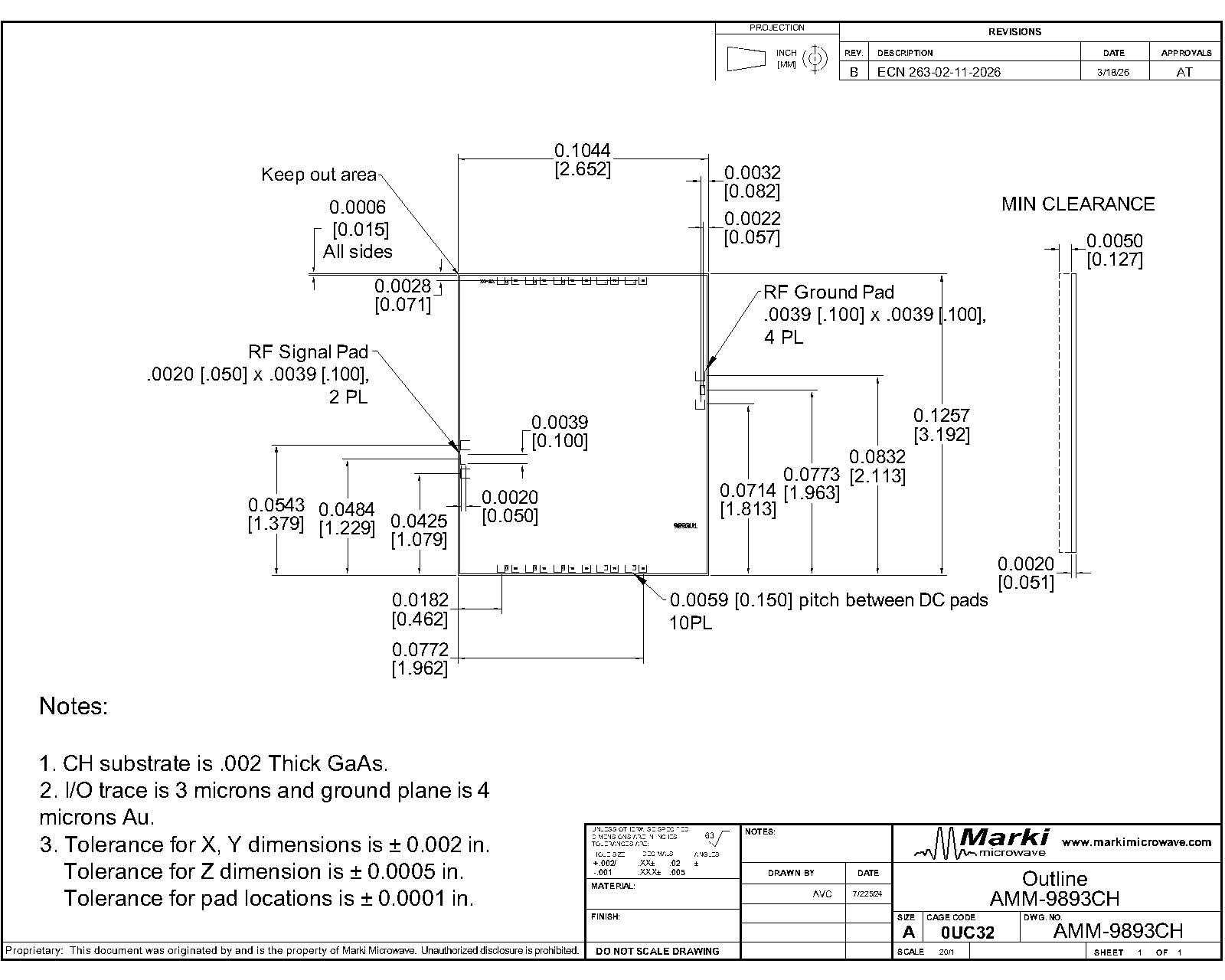

Port Diagram
The port diagram of the AMM-9893CH is shown below. There are two sets of DC pads, one on the North and one on the South edge of the die. They perform identical functions and are internally connected on the die. They are provided for convenience in bias routing and only one pad of each type needs to be connected.


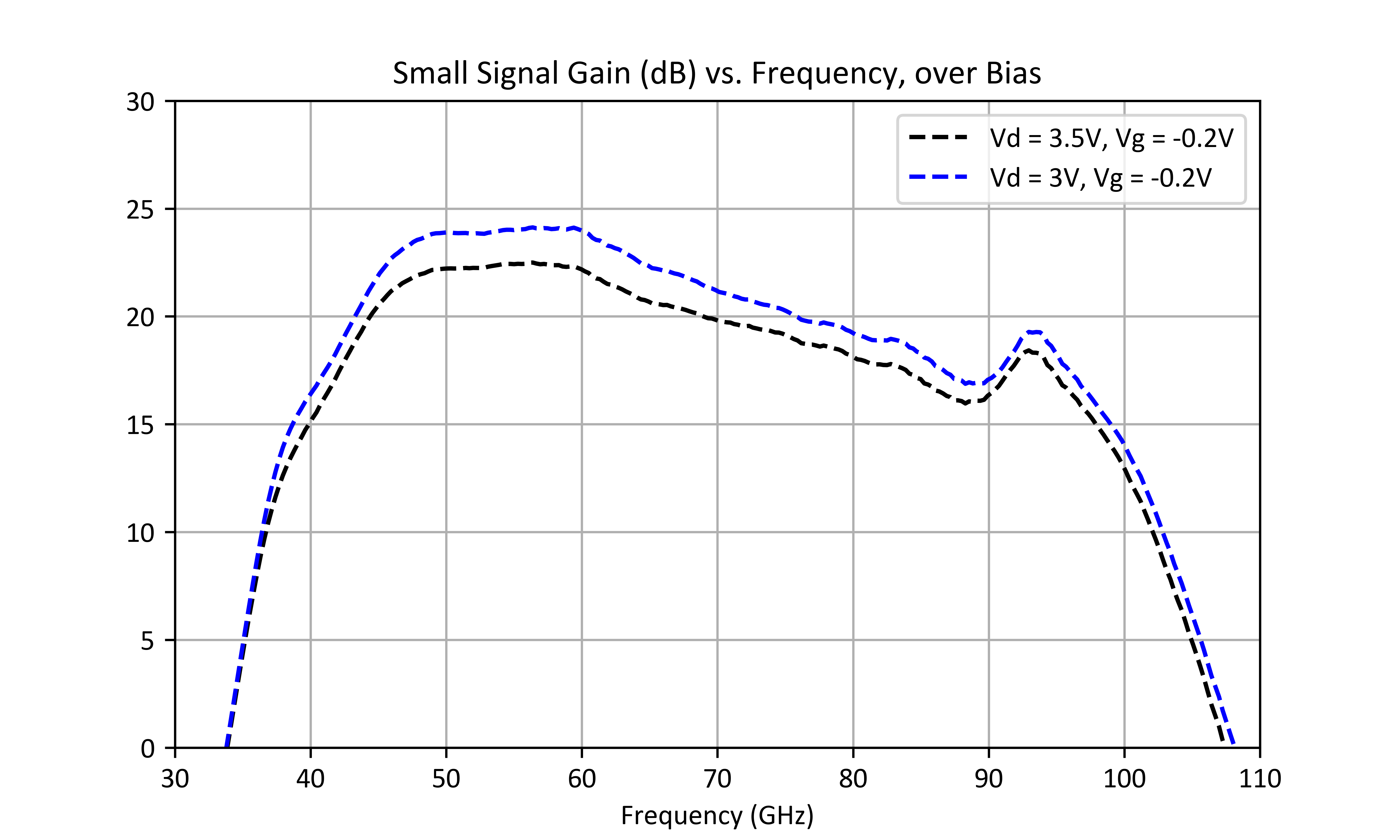%20vs.%20Frequency,%20over%20Bias.png)
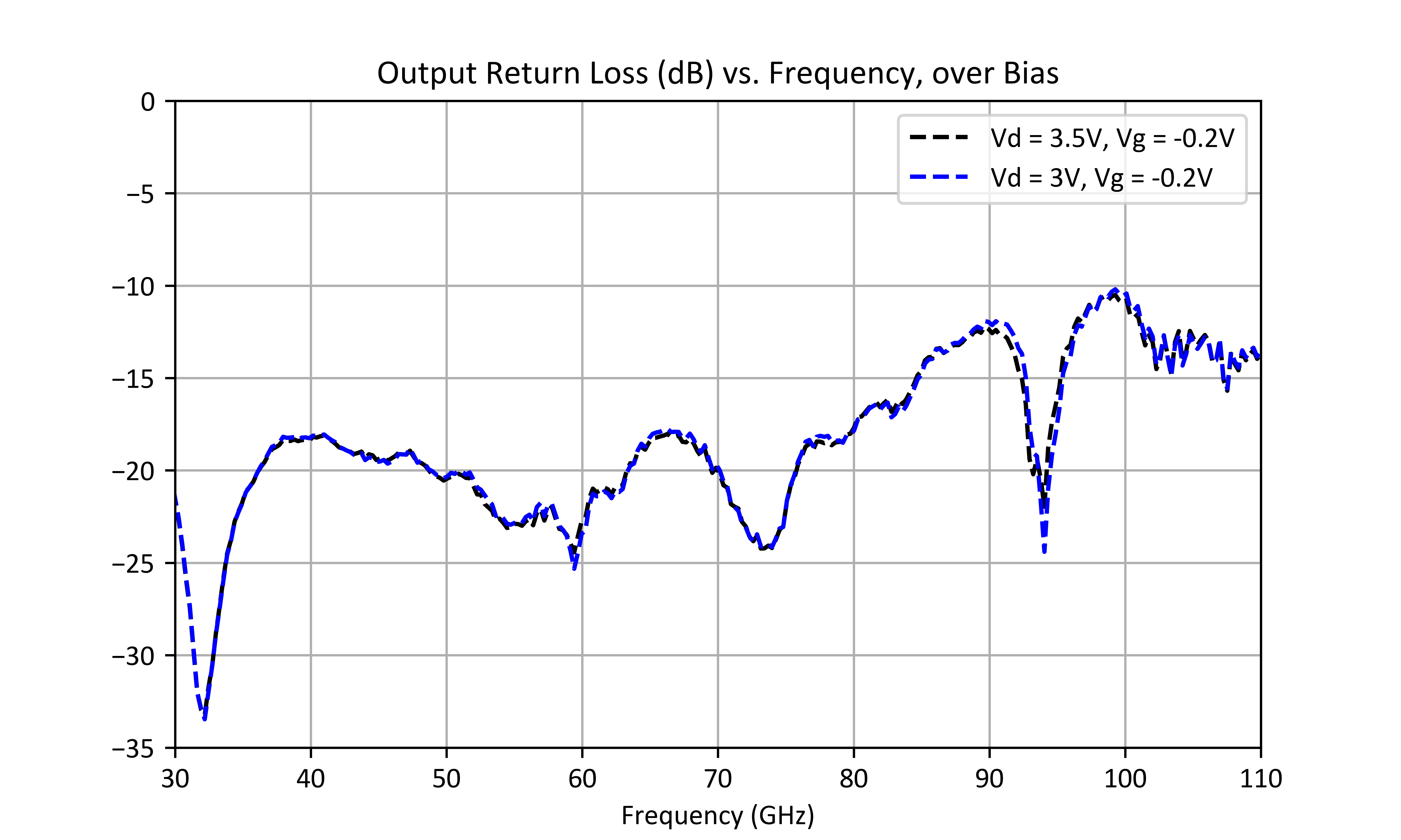%20vs.%20Frequency,%20over%20Bias.png)
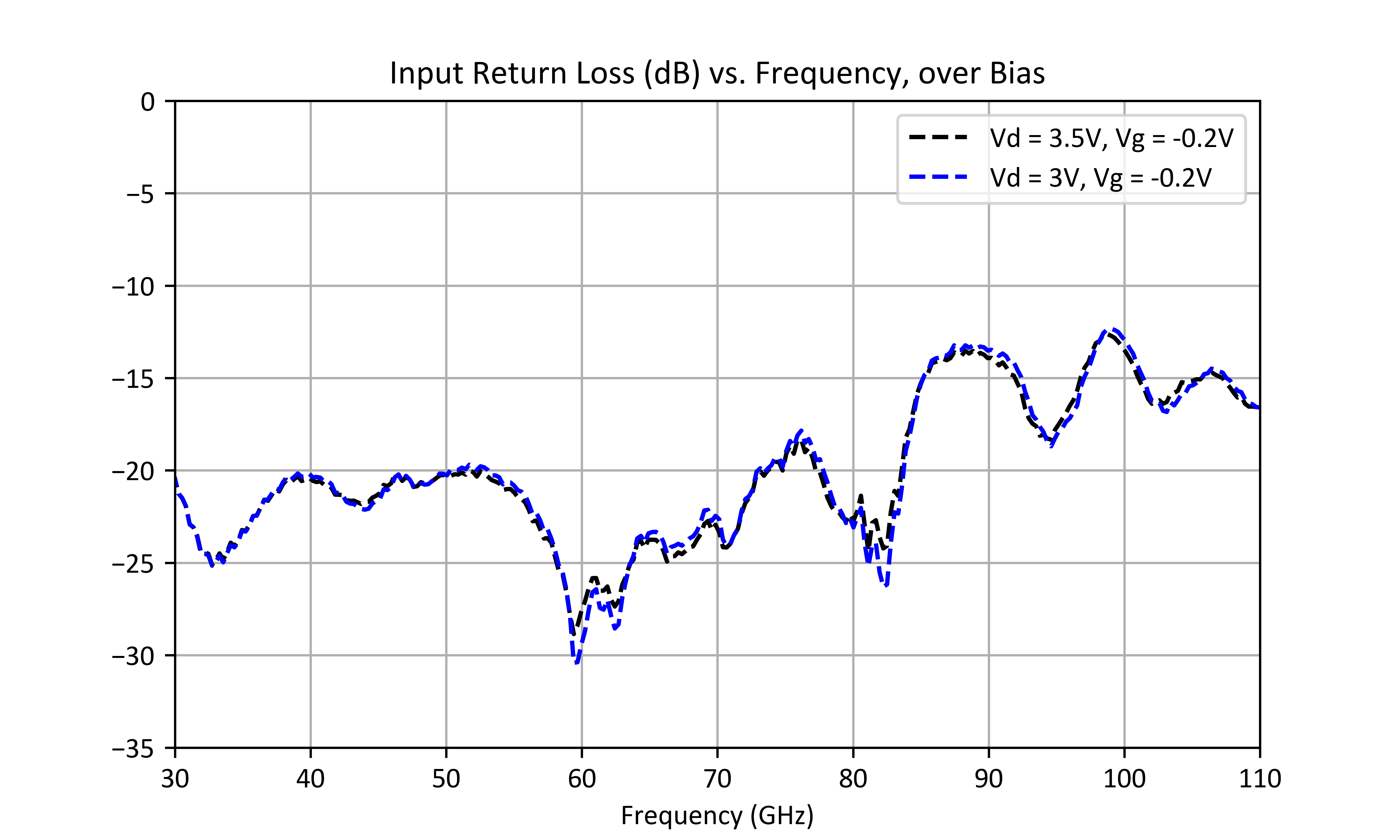%20vs.%20Frequency,%20over%20Bias.png)