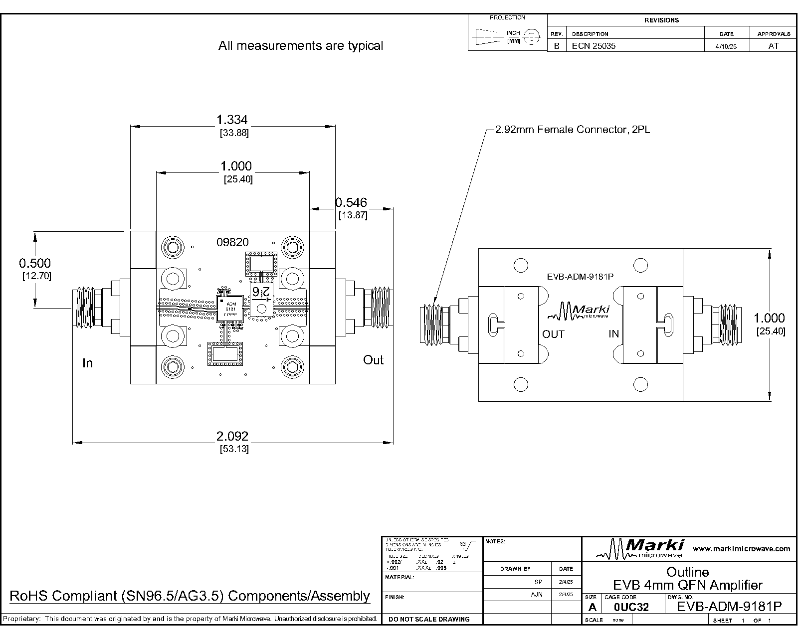
Port Diagram

Sales: 408-778-9952 | General: 408-778-4200 | Fax: 408-778-4300
Sales & Customer Support: [email protected]
Tech Support: [email protected]
The ADM-9181CH is a wideband distributed amplifier capable of providing 14.5 dB gain and +31 dBm OIP3 from 100MHz to 22 GHz. The ADM-9181CH is an ideal linear signal amplifier for applications requiring low power consumption and small form-factors. The amplifier has excellent return losses and gain flatness.

| Part Number | Description | Package | Green Status | Product Lifecycle | Export Classification |
|---|---|---|---|---|---|
| ADM-9181CH | DC - 26 GHz Distributed Amplifier | CH | RoHS | Released | EAR99 |
| Part Number | Description | Package | Green Status | Product Lifecycle | Export Classification |
|---|---|---|---|---|---|
| ADM-9181CH | DC - 26 GHz Distributed Amplifier | CH | RoHS | Released | EAR99 |
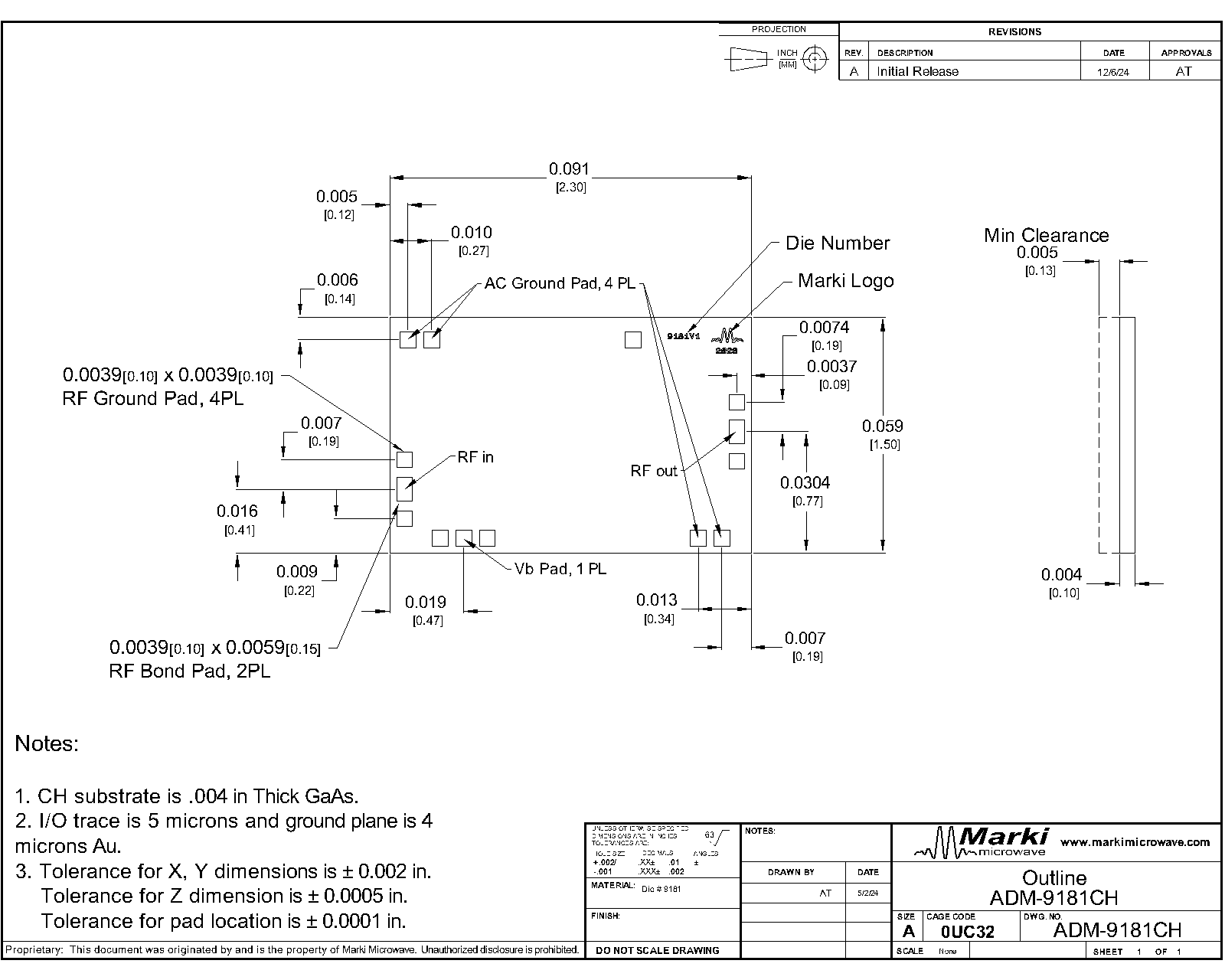
ADM-9181CH
DC - 26 GHz Distributed Amplifier
| Revision Code | Revision Date | Comment |
|---|---|---|
| - | 2024-08-29 | Initial Release |
ADM-9181CH
DC - 26 GHz Distributed Amplifier
ADM-9181CH
DC - 26 GHz Distributed Amplifier
| Port | Function | Description | DC Equivalent Circuit |
|---|---|---|---|
| ACG1 | External Chip Capacitor | The ACG1 pad provides additional off chip bypass capacitance. A 0.1uF chip capacitor is recommended. |  |
| ACG2 | External Chip Capacitor | The ACG2 pad provides additional off chip bypass capacitance. A 100pF chip capacitor is recommended. | |
| ACG3 | External Chip Capacitor | The ACG3 pad provides additional off chip bypass capacitance. A 100pF chip capacitor is recommended. | |
| ACG4 | External Chip Capacitor | The ACG4 pad provides additional off chip bypass capacitance. A 0.1uF chip capacitor is recommended. | |
| GND | Gnd | Gnd is provided through the backside of the die and should be connected to a DC/RF ground potential with high thermal and electrical conductivity. |  |
| RF In | RF Input | This is the amplifier’s RF Input port. It is RF matched to 50 Ω and requires a DC blocking capacitor. |  |
| RF Out / Vd | RF Out / Vd | The RF Out/ Vd pad supplies DC voltage to the drain of the amplifier IC and also acts as the RF output. This pad requires an external bias-tee. Nominal voltage for Vd at this pad is +6V. |  |
| Vb | Positive bias | The Vb pad provides a required positive bias which supplies an internal current mirror. A higher voltage results in higher current draw through the VD / RF Out port. This port should be set to +3V for normal operation. |  |
ADM-9181CH
DC - 26 GHz Distributed Amplifier
The Absolute Maximum Ratings indicate limits beyond which damage may occur to the device. If any one of these limits are exceeded, the device may become inoperable or have a reduced lifetime. Reliability limits are individual, instantaneous catastrophic limits only. Functional operation limits are indicated below. Operation of the device at multiple absolute maximum limits or for extended periods at a single limit can cause degradation and damage to the device.
| Parameter | Maximum Rating | Unit |
|---|---|---|
| Bias Supply Voltage (Vb) | 6.5 | V |
| Drain Current (Id) (No RF Applied) | 250 | mA |
| Maximum Operating Temperature for MTTF > 1E6 hours | 85 | °C |
| Maximum Storage Temperature | 125 | °C |
| Minimum Operating Temperature for MTTF > 1E6 hours | -40 | °C |
| Minimum Storage Temperature | -65 | °C |
| Positive Drain Supply Voltage (Vd) | 8 | V |
| RF Input Power | 20 | dBm |
| Parameter | Details | Rating |
|---|---|---|
| Dimensions | - | 2.3 x 1.5 mm |
The Recommended Operating Conditions indicate the limits, inside which the device should be operated, to guarantee the performance given in Electrical Specifications Operating outside these limits may not necessarily cause damage to the device, but the performance may degrade outside the limits of the electrical specifications. For limits, above which damage may occur, see Absolute Maximum Ratings.
| Parameter | Min | Nominal | Max | Unit |
|---|---|---|---|---|
| Positive DC Current (Id) (No RF Input) | 82 | 130 | 190 | mA |
| Positive DC Bias Voltage (Vb) | 2 | 3 | 4.4 | V |
| Ambient Temperature | -40 | 25 | 85 | °C |
| Positive DC Voltage (Vd) | 4 | 5 | 6 | V |
ADM-9181CH
DC - 26 GHz Distributed Amplifier
| Parameter | Test Conditions | Minimum Frequency (GHz) | Maximum Frequency (GHz) | Min | Typ | Max | Unit |
|---|---|---|---|---|---|---|---|
| Input IP2 1 | Vd = 6V, Vb = 3V, Pin = -20dBm | 0.1 | 13 | - | 24 | - | dBm |
| Input IP3 | Vd = 6V, Vb = 3V, Pin = -20dBm | 0.1 | 26 | - | 17 | - | dBm |
| Input Return Loss | Vd = 6V, Vb = 3V, Pin = -20dBm | 0.1 | 26 | - | 19 | - | dB |
| Noise Figure | Vd = 6V, Vb = 3V, Pin = -20dBm | 6 | 26 | - | 3.4 | - | dB |
| Noise Figure | Vd = 6V, Vb = 3V, Pin = -20dBm | 0.1 | 6 | - | 6 | - | dB |
| Output IP2 2 | Vd = 6V, Vb = 3V, Pin = -20dBm | 0.1 | 13 | - | 38 | - | dBm |
| Output IP3 | Vd = 6V, Vb = 3V, Pin = -20dBm | 0.1 | 26 | - | 31 | - | dBm |
| Output P1dB | Vd = 6V, Vb = 3V | 0.1 | 20 | - | 22 | - | dBm |
| Output P1dB | Vd = 6V, Vb = 3V | 20 | 26 | - | 18.5 | - | dBm |
| Output Return Loss | Vd = 6V, Vb = 3V, Pin = -20dBm | 0.1 | 26 | - | 23 | - | dB |
| Reverse Isolation | Vd = 6V, Vb = 3V, Pin = -20dBm | 0.1 | 26 | - | 38 | - | dB |
| Small Signal Gain | Vd = 6V, Vb = 3V, Pin = -20dBm | 0.1 | 26 | - | 14.5 | - | dB |
[1][2] IP2 is specified up to an input frequency of 13GHz where the IM2 product becomes attenuated by the frequency response of the amplifier.
ADM-9181CH
DC - 26 GHz Distributed Amplifier
%20vs.%20Frequency,over%20Bias.png)
%20vs.%20Frequency,over%20Bias.png)
%20vs.%20Frequency,%20over%20Bias.png)
%20vs.%20Frequency,%20over%20Bias.png)
%20vs.%20Frequency,over%20Bias.png)
%20vs.%20Frequency,over%20Bias.png)
%20vs.%20Frequency,over%20Bias.png)
%20vs.%20Frequency,over%20Bias.png)
ADM-9181CH
DC - 26 GHz Distributed Amplifier
%20vs.%20Frequency,over%20Bias.png)
%20vs.%20Frequency,over%20Bias.png)
ADM-9181CH
DC - 26 GHz Distributed Amplifier

ADM-9181CH
DC - 26 GHz Distributed Amplifier
Download : Outline 2D Drawing
Notes:
ADM-9181CH
DC - 26 GHz Distributed Amplifier