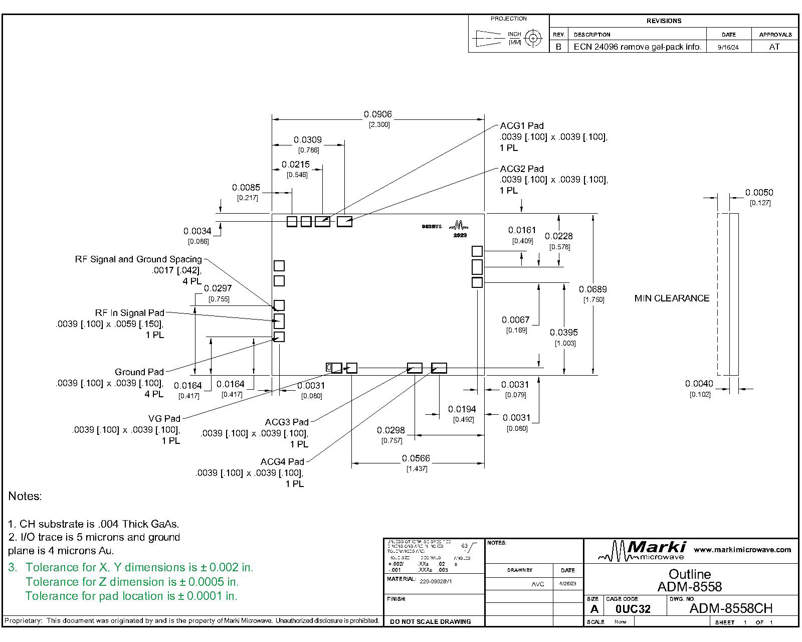
Port Diagram

Sales: 408-778-9952 | General: 408-778-4200 | Fax: 408-778-4300
Sales & Customer Support: [email protected]
Tech Support: [email protected]
The ADM-8558 is a wideband distributed low noise amplifier capable of providing 16 dB gain and +23 dBm OIP3 from DC to 20 GHz and a low 1.8 dB typical noise figure from 7 to 15 GHz. The ADM-8558 is an ideal linear signal amplifier for applications requiring low power consumption and small form-factors. ADM-8558 is available in bare die and connectorized module forms. The amplifier has excellent return losses and gain flatness.


| Part Number | Description | Package | Connectors | Green Status | Product Lifecycle | Export Classification |
|---|---|---|---|---|---|---|
| ADM-8558PC | 0.005 - 20 GHz Distributed Amplifier | PC | Standard | RoHS REACH | Released | EAR99 |
| ADM-8558CH | DC - 20 GHz Distributed Amplifier | CH | - | RoHS REACH | Released | EAR99 |
ADM-8558CH
DC - 20 GHz Distributed Amplifier
| Revision Code | Revision Date | Comment |
|---|---|---|
| - | 2023-07-01 | Datasheet Initial Release |
| A | 2024-08-02 | Updated according to ECN# 24031. Updated voltage limits, performance plots, application circuit and outline drawing. |
ADM-8558CH
DC - 20 GHz Distributed Amplifier
ADM-8558CH
DC - 20 GHz Distributed Amplifier
| Port | Function | Description | DC Equivalent Circuit |
|---|---|---|---|
| ACG1 | External Chip Capacitor | The ACG1 pad provides additional off chip bypass capacitance. A 100pF chip capacitor is recommended. |  |
| ACG2 | External Chip Capacitor | The ACG2 pad provides additional off chip bypass capacitance. A 0.1uF chip capacitor is recommended. | |
| ACG3 | External Chip Capacitor | The ACG3 pad provides additional off chip bypass capacitance. A 0.1uF chip capacitor is recommended. | |
| ACG4 | External Chip Capacitor | The ACG4 pad provides additional off chip bypass capacitance. A 100pF chip capacitor is recommended. | |
| GND | Ground | Housing or ground lug must be connected to a DC/RF ground potential with high thermal and electrical conductivity. |  |
| RF In | RF Input | This is the amplifier’s RF Input port. It is RF matched to 50 Ω and requires an DC blocking capacitors |  |
| Vd/RF Out | Drain Supply / RF Output | The VD pin supplies DC voltage to the drain of the amplifier IC. This pin is nominally set at +6V. |  |
| Vg | Gate Bias Pin | The VG pad provides a required positive bias which supplies the current mirror. A higher voltage results in a higher current draw through the VD / RF Out port. This port should be set to +3V for normal operation. |  |
ADM-8558CH
DC - 20 GHz Distributed Amplifier
The Absolute Maximum Ratings indicate limits beyond which damage may occur to the device. If these limits are exceeded, the device may become inoperable or have a reduced lifetime. Reliability limits are individual, instantaneous catastrophic limits only. Functional operation limits are indicated below. Operation of the device at multiple absolute maximum limits or for extended periods at a single limit can cause degradation and damage to the device
| Parameter | Maximum Rating | Unit |
|---|---|---|
| Drain Current (Id) (No RF Applied) | 80 | mA |
| Drain Supply Voltage (Vd) | 8.5 | V |
| Gate Current (Ig) | 10 | mA |
| Gate Supply Voltage (Vg) | 6.5 | V |
| Maximum Operating Temperature for MTTF > 1E6 hours | 85 | °C |
| Maximum Storage Temperature | 125 | °C |
| Minimum Operating Temperature for MTTF > 1E6 hours | -40 | °C |
| Minimum Storage Temperature | -55 | °C |
| RF Power Handling | 15 | dBm |
| Parameter | Details | Rating |
|---|---|---|
| Dimensions | - | 1.75 x 2.3 mm |
The Recommended Operating Conditions indicate the limits, inside which the device should be operated, to guarantee the performance given in Electrical Specifications. Operating outside these limits may not necessarily cause damage to the device, but the performance may degrade outside the limits of the electrical specifications. For limits, above which damage may occur, see Absolute Maximum Ratings.
| Parameter | Min | Nominal | Max | Unit |
|---|---|---|---|---|
| Ambient Temperature | -40 | 25 | 85 | °C |
| Power Supply DC Voltage (Vd) | 6 | 6 | 8 | V |
| Power Supply DC Current (Id) (No RF Input) | 50 | 50 | 70 | mA |
| Gate Bias DC Voltage (Vg) | 3 | 3 | 4 | V |
ADM-8558CH
DC - 20 GHz Distributed Amplifier
Unless otherwise specified, electrical specifications apply at TA=+25°C, Vd = 6V, Vg = 3V.
| Parameter | Test Conditions | Minimum Frequency (GHz) | Maximum Frequency (GHz) | Min | Typ | Max | Unit |
|---|---|---|---|---|---|---|---|
| Saturated Output Power | - | 2 | 24 | - | 19 | - | dBm |
| Current Consumption | Vd = 6V,
Vg = 3V,
No RF input | 0.004 | 20 | - | 50 | - | mA |
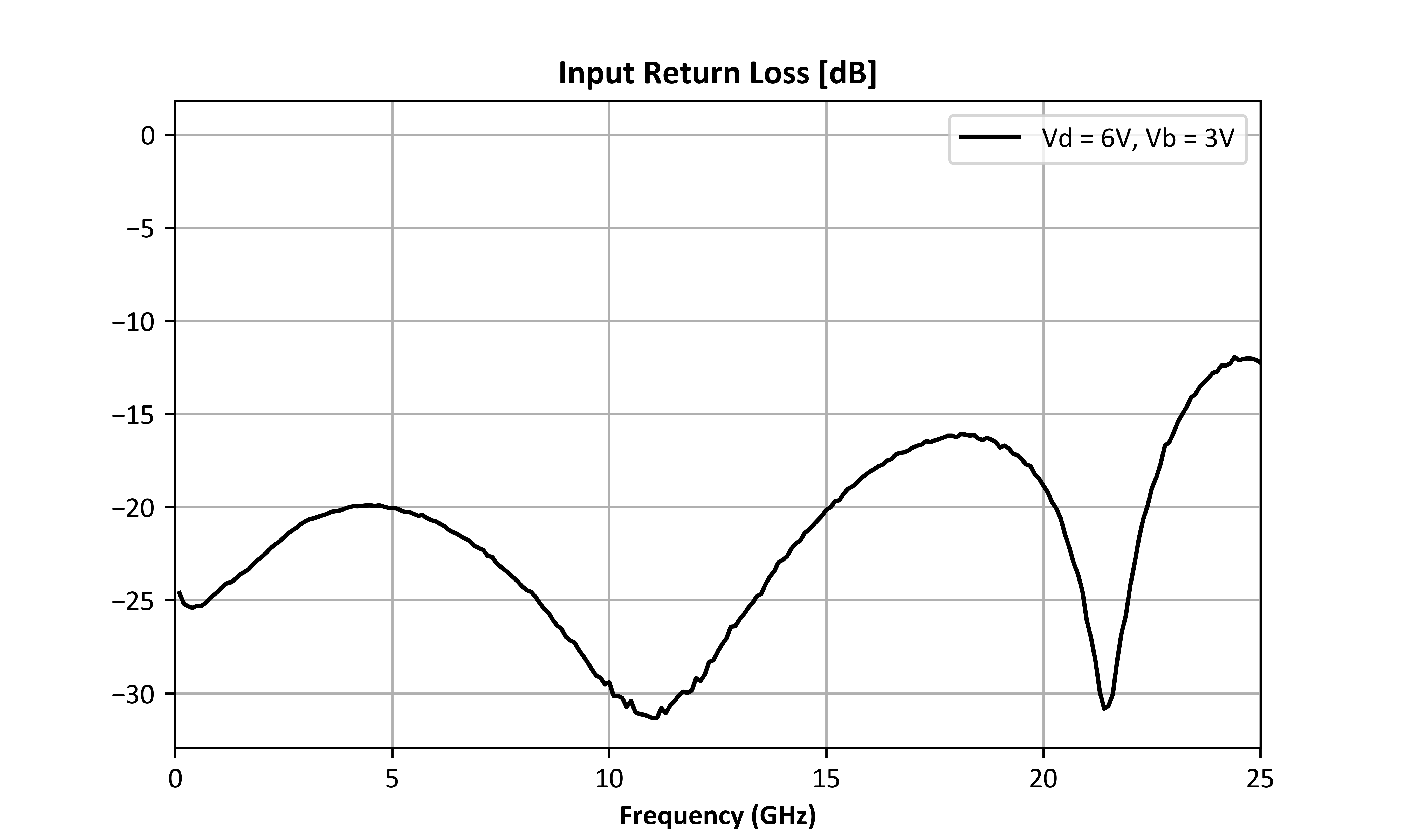
| Input Return Loss | Vd = 6V,
Vg = 3V,
Pin = -20dBm | 0.005 | 20 | - | 21 | - | dB |
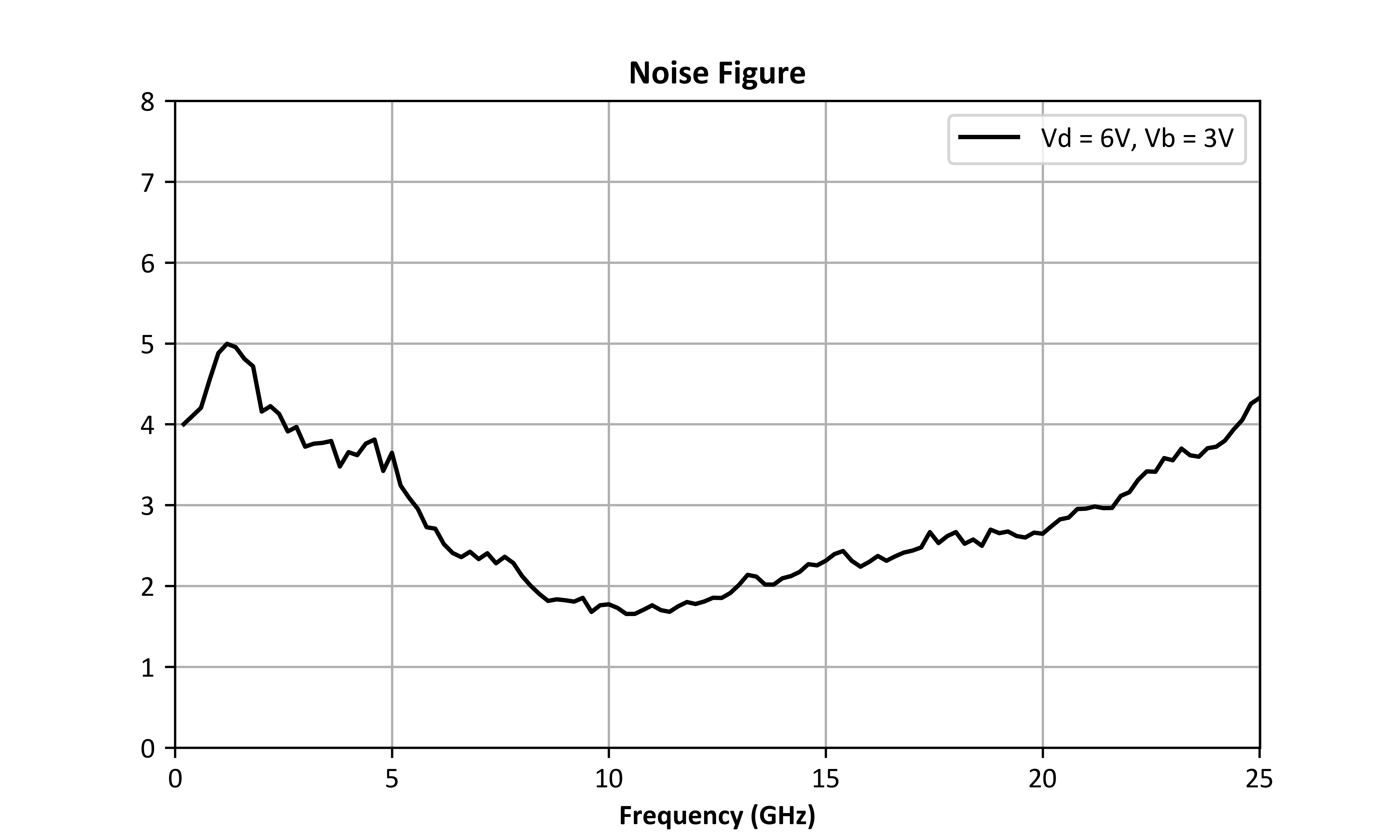
| Noise Figure | Vd = 6V,
Vg = 3V,
Pin = -20dBm | 0.005 | 7 | - | 3.8 | - | dB |
| Noise Figure | Vd = 6V,
Vg = 3V,
Pin = -20dBm | 15 | 20 | - | 2.8 | - | dB |
| Noise Figure | Vd = 6V,
Vg = 3V,
Pin = -20dBm | 7 | 15 | - | 1.8 | - | dB |
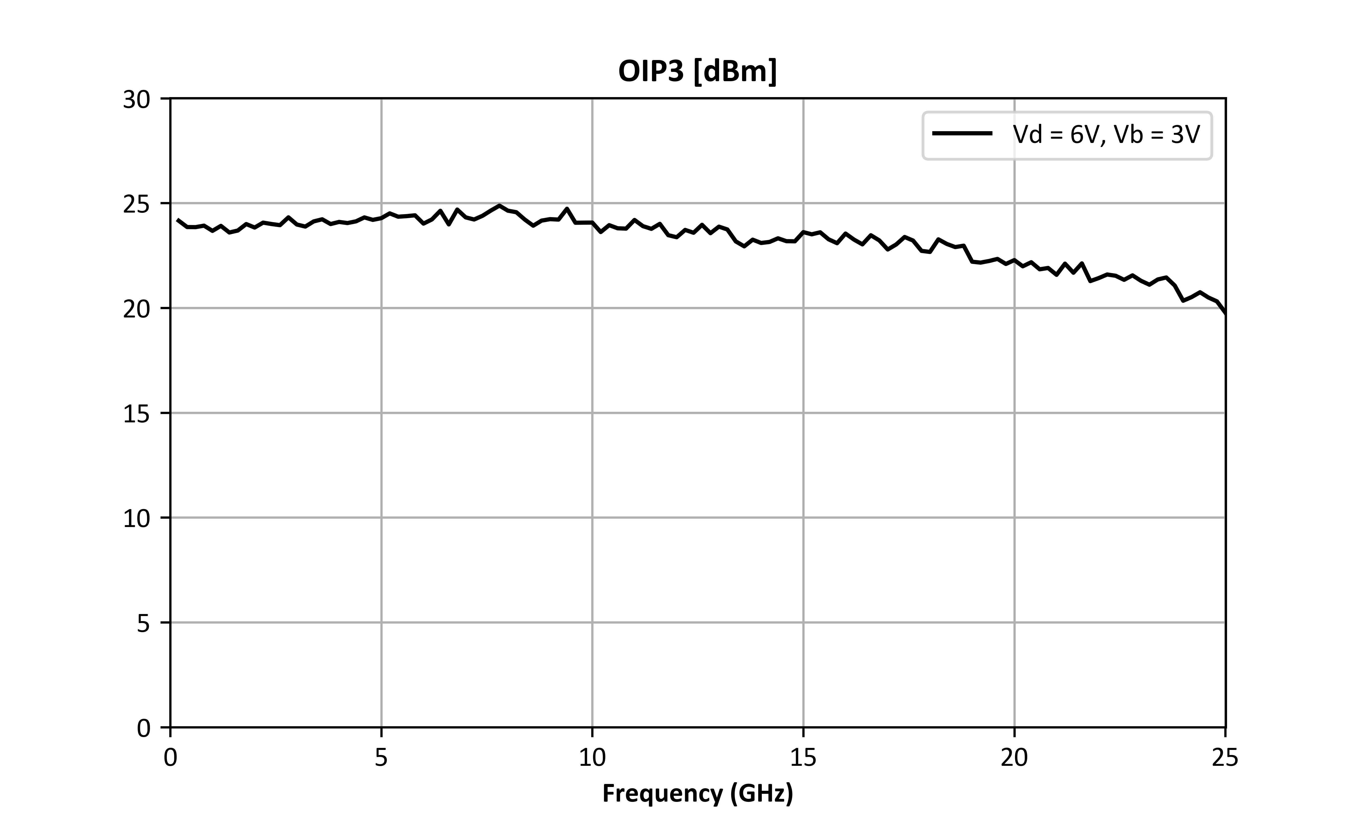
| Output IP3 | Vd = 6V,
Vg = 3V,
Pin = -20dBm | 0.004 | 20 | - | 23 | - | dBm |
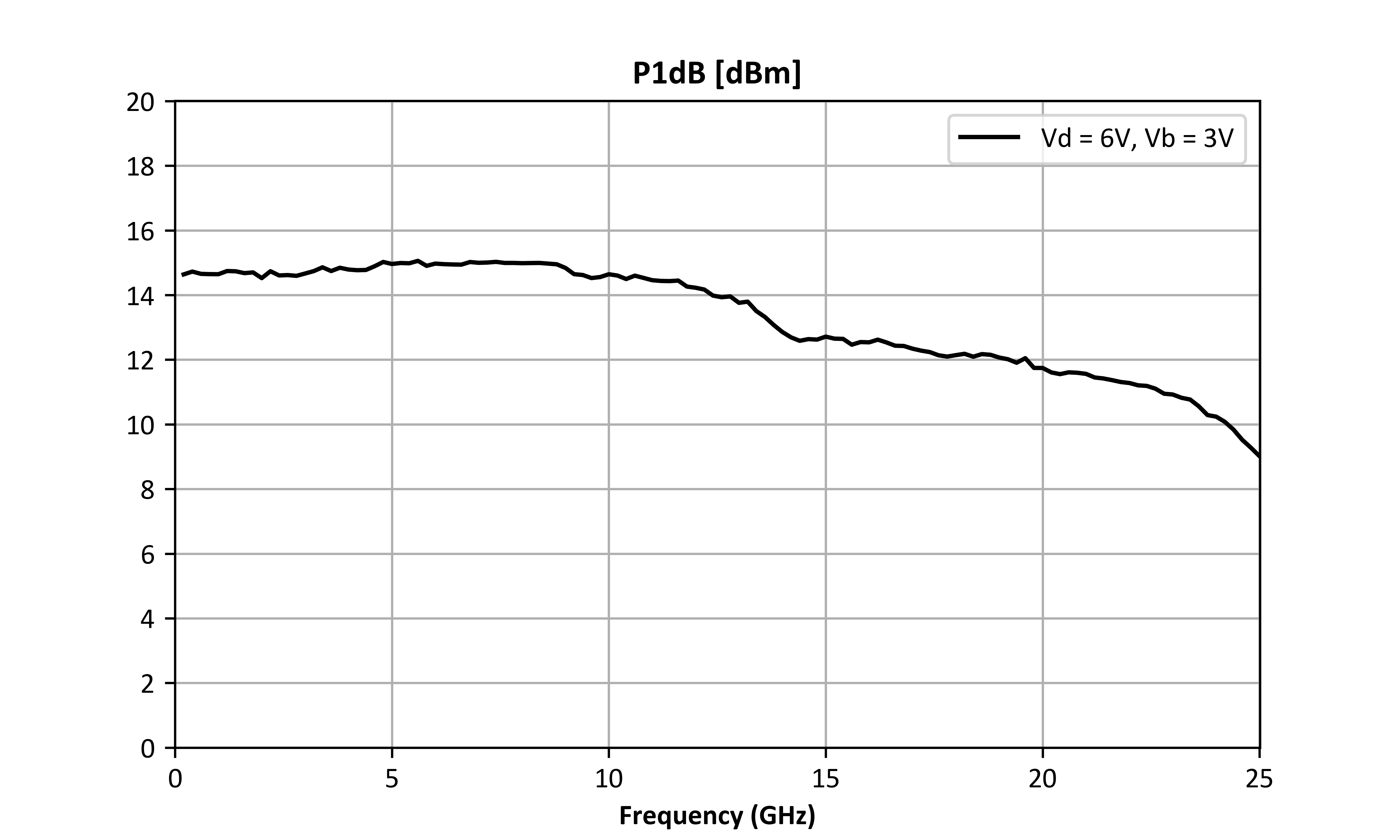
| Output P1dB | Vd = 6V,
Vg = 3V | 0.005 | 20 | - | 14 | - | dBm |
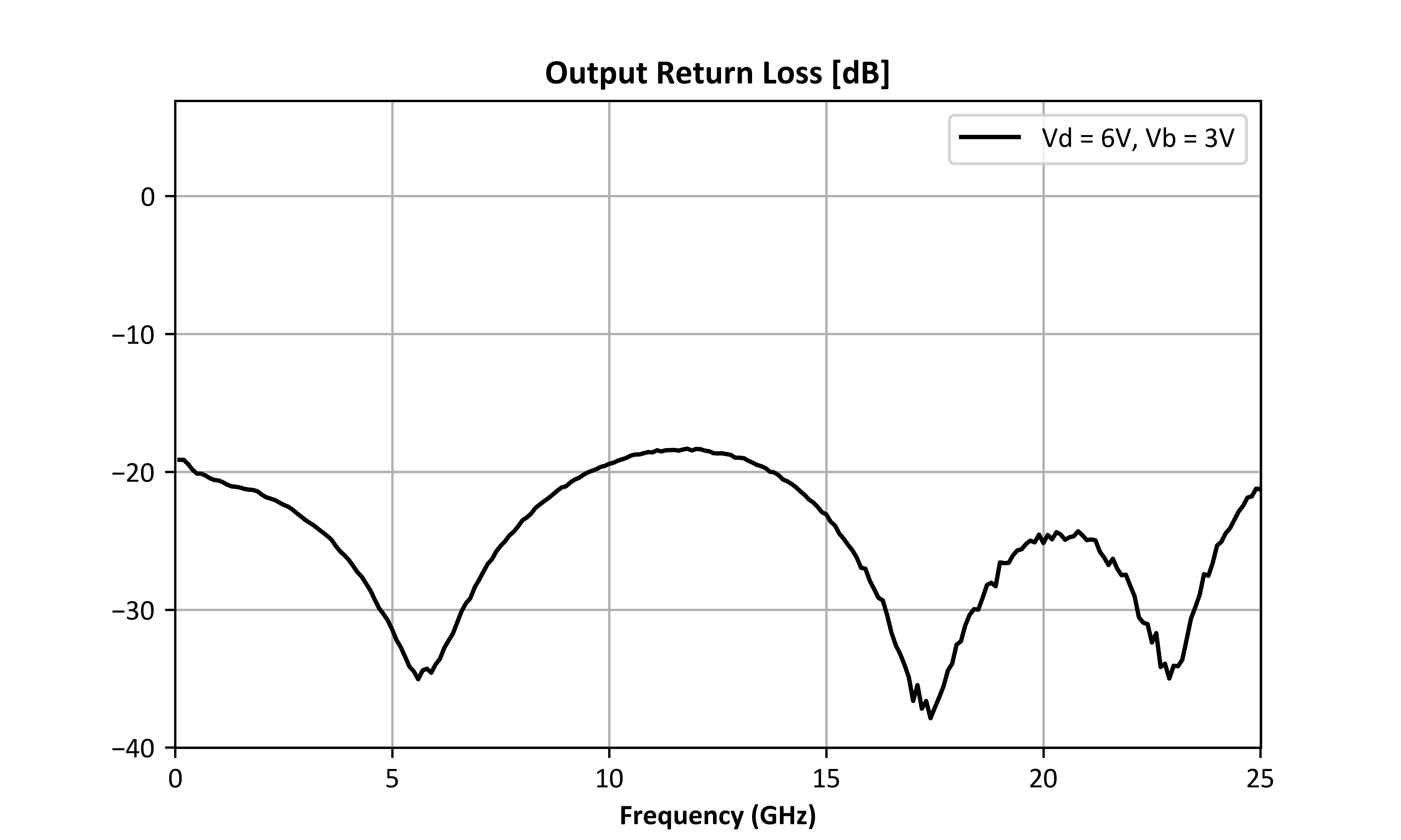
| Output Return Loss | Vd = 6V,
Vg = 3V,
Pin = -20dBm | 0.004 | 20 | - | 23 | - | dB |
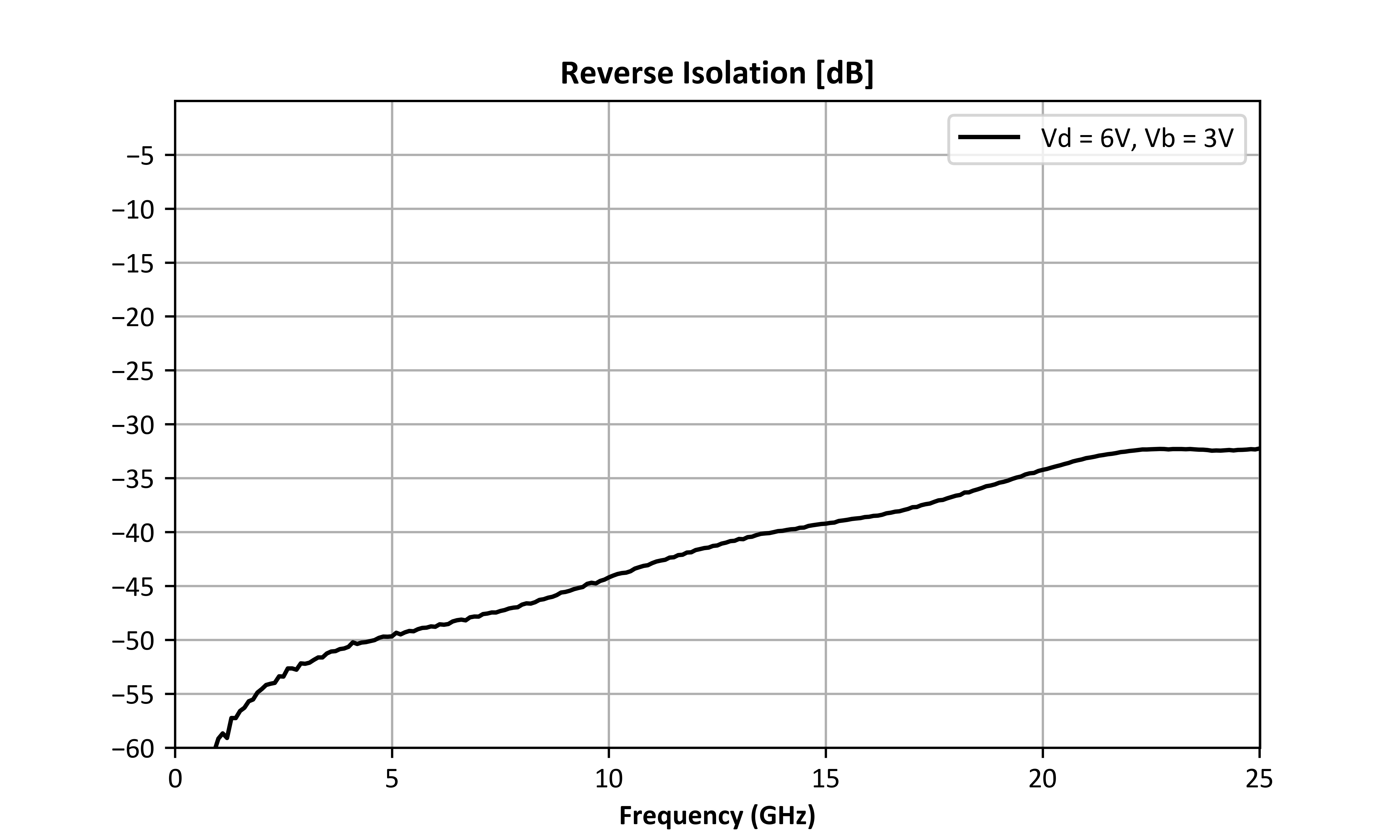
| Reverse Isolation | Vd = 6V,
Vg = 3V,
Pin = -20dBm | 0.004 | 20 | - | 40 | - | dB |
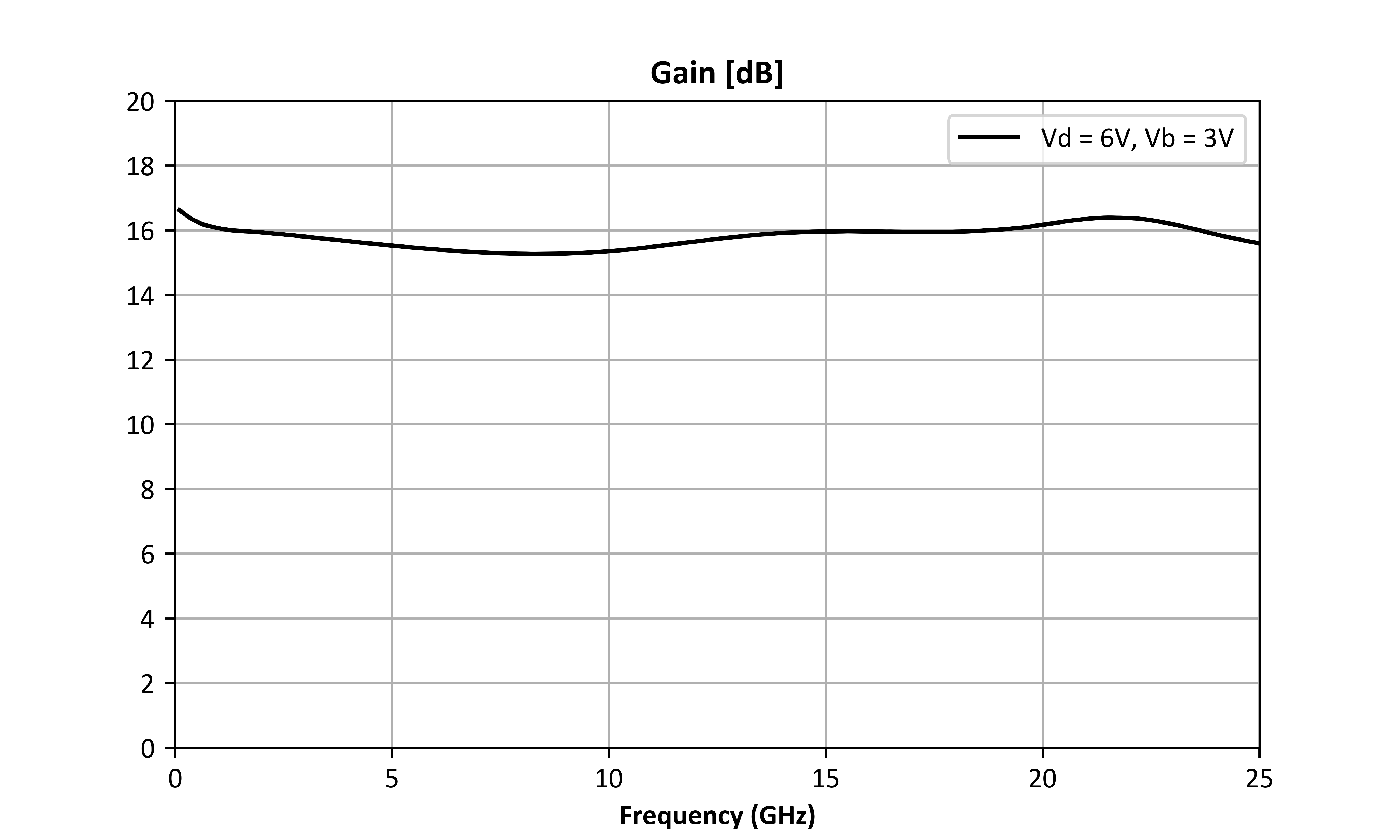
| Small Signal Gain | Vd = 6V,
Vg = 3V,
Pin = -20dBm | 0.005 | 20 | 14 | 16 | - | dB |
| Parameter | Test Conditions | Minimum Frequency (GHz) | Maximum Frequency (GHz) | Min | Typ | Max | Unit |
|---|---|---|---|---|---|---|---|
| Saturated Output Power | - | 2 | 24 | - | 19 | - | dBm |
| Current Consumption | Vd = 6V,
Vg = 3V,
No RF input | 0.004 | 20 | - | 50 | - | mA |
| Input Return Loss | Vd = 6V,
Vg = 3V,
Pin = -20dBm | 0.005 | 20 | - | 21 | - | dB |
| Noise Figure | Vd = 6V,
Vg = 3V,
Pin = -20dBm | 0.005 | 7 | - | 3.8 | - | dB |
| Noise Figure | Vd = 6V,
Vg = 3V,
Pin = -20dBm | 15 | 20 | - | 2.8 | - | dB |
| Noise Figure | Vd = 6V,
Vg = 3V,
Pin = -20dBm | 7 | 15 | - | 1.8 | - | dB |
| Output IP3 | Vd = 6V,
Vg = 3V,
Pin = -20dBm | 0.004 | 20 | - | 23 | - | dBm |
| Output P1dB | Vd = 6V,
Vg = 3V | 0.005 | 20 | - | 14 | - | dBm |
| Output Return Loss | Vd = 6V,
Vg = 3V,
Pin = -20dBm | 0.004 | 20 | - | 23 | - | dB |
| Reverse Isolation | Vd = 6V,
Vg = 3V,
Pin = -20dBm | 0.004 | 20 | - | 40 | - | dB |
| Small Signal Gain | Vd = 6V,
Vg = 3V,
Pin = -20dBm | 0.005 | 20 | 14 | 16 | - | dB |
ADM-8558CH
DC - 20 GHz Distributed Amplifier
ADM-8558CH
DC - 20 GHz Distributed Amplifier
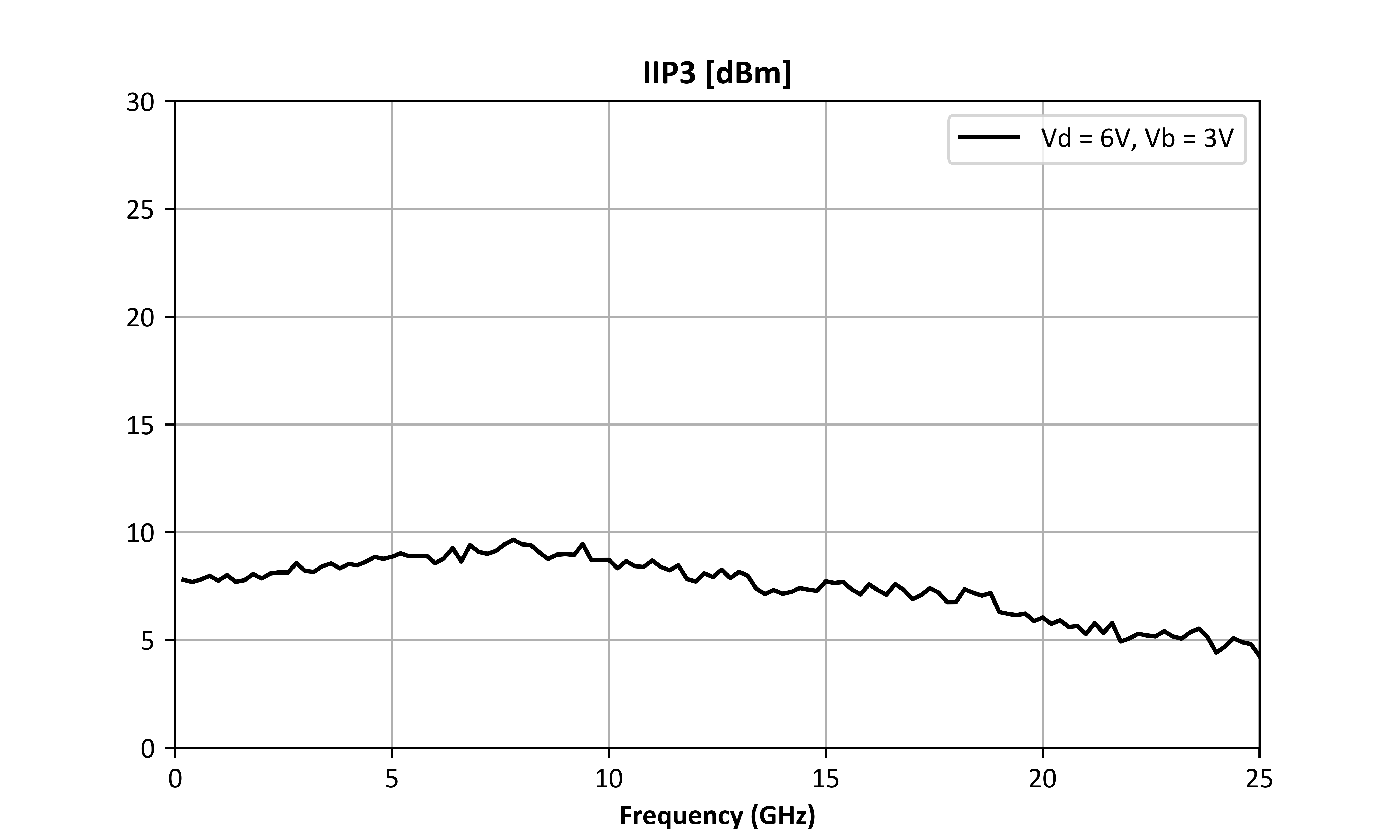
Performance plots for the connectorized module are shown for measurements where directly probed measurements of the die are unavailable. Note that the following measurements include losses from connectors and microstrip traces.
%20vs.%20Frequency,%20over%20Bias.png)
%20vs.%20Frequency,%20over%20Bias.png)
%20vs.%20Frequency,%20over%20Bias.png)
%20vs.%20Frequency,%20over%20Bias.png)
%20vs.%20Frequency,%20over%20Bias.png)
%20vs.%20Frequency,%20over%20Bias.png)
%20vs.%20Frequency,%20over%20Bias.png)
%20vs.%20Frequency,%20over%20Bias.png)
ADM-8558CH
DC - 20 GHz Distributed Amplifier
%20vs.%20Frequency,%20over%20Bias.png)
%20vs.%20Frequency,%20over%20Temperature%20at%20Vd%20=%206V,%20Vb%20=%203V.png)
%20vs.%20Frequency,%20over%20Temperature%20at%20Vd%20=%206V,%20Vb%20=%203V.png)
%20vs.%20Frequency,%20over%20Temperature%20at%20Vd%20=%206V,%20Vb%20=%203V.png)
%20vs.%20Frequency,%20over%20Bias.png)
%20vs.%20Pin,%20over%20Frequency%20at%20Vd%20=%206.png)
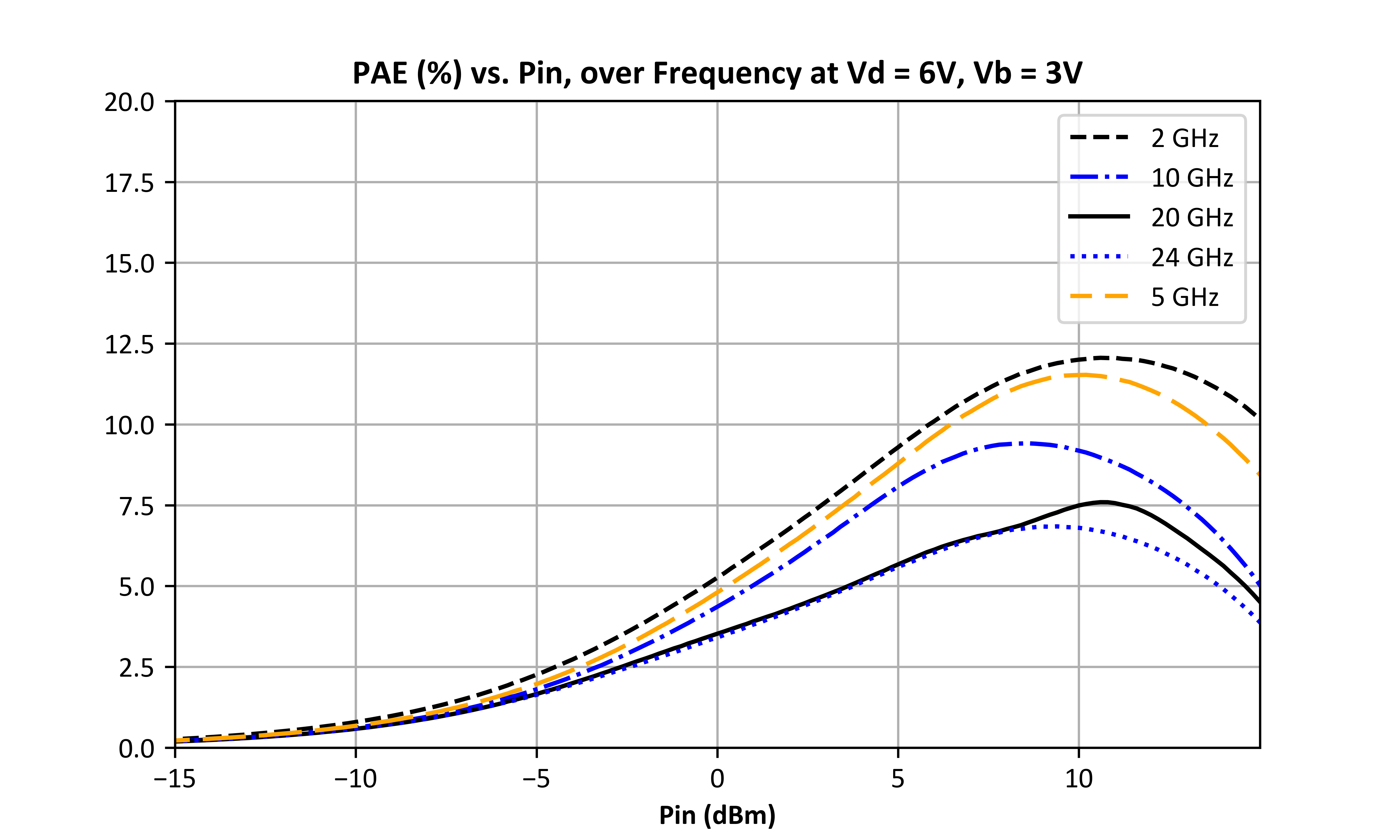
%20vs.%20Pin,%20over%20Frequency%20at%20Vd%20=%206.png)
ADM-8558CH
DC - 20 GHz Distributed Amplifier

ADM-8558CH
DC - 20 GHz Distributed Amplifier
Download : Outline 2D Drawing
Notes: