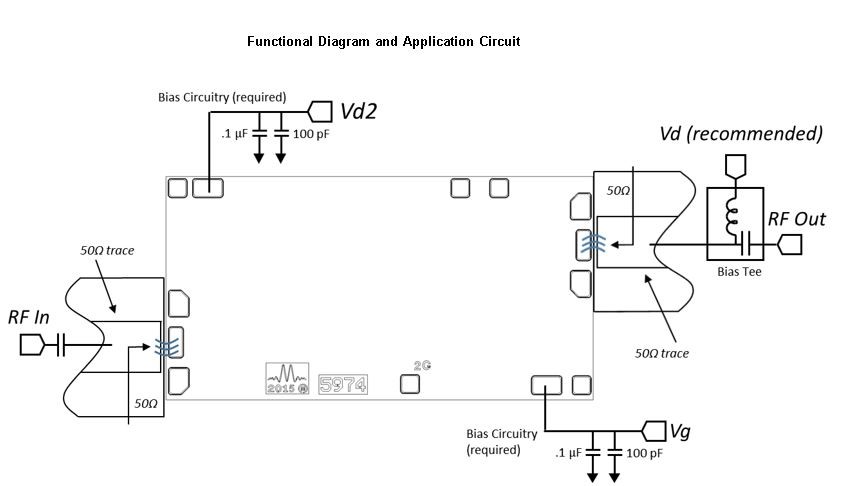
Port Diagram
Sales: 408-778-9952 | General: 408-778-4200 | Fax: 408-778-4300
Sales & Customer Support: [email protected]
Tech Support: [email protected]
The ADM-5974CH is a broadband, moisture resistant MMIC LO buffer amplifier. The ADM-5974 provides efficient, optimized LO drive to all Marki mixers in band with no required negative bias or sequencing. It is built with a moisture resistant pHEMT process to allow the bare chip to pass biased HAST testing without a hermetic seal. Second harmonic rejection can be tuned to very low levels using the optional negative bias. The ADM-5974 can also be used as a broadband signal amplifier. The bare die features enhanced moisture resistance for improved reliability.

N/A

| Part Number | Description | Package | Green Status | Product Lifecycle | Export Classification |
|---|---|---|---|---|---|
| ADM-5974CH | Broadband Distributed Amplifier | CH | REACH RoHS | Released | 3A001.b.2.d |
| Part Number | Description | Package | Green Status | Product Lifecycle | Export Classification |
|---|---|---|---|---|---|
| ADM-5974CH | Broadband Distributed Amplifier | CH | REACH RoHS | Released | 3A001.b.2.d |
ADM-5974CH
Broadband Distributed Amplifier
| Revision Code | Revision Date | Comment |
|---|---|---|
| - | 2017-04-01 | Datasheet initial Release |
| A | 2019-07-01 | Thermal Resistance Spec Corrected |
| B | 2020-12-01 | Added Max Junction Temperature Specification |
ADM-5974CH
Broadband Distributed Amplifier
| Port | Function | Description | DC Equivalent Circuit |
|---|---|---|---|
| GND | Gnd | Back of chip should be connected to RF/DC ground with low electrical and thermal resistance. |  |
| RF In | RF Input | This pin is DC coupled and matched to 50 Ω. |  |
| Vd2 | Vd2 | Optional drain bias port. External decoupling capacitors are required. |  |
| Vd/RF Out | RF Out / Vd | This pad is DC coupled and matched to 50 Ω. |  |
| Vg | Vg | Gate control for the amplifier. External decoupling capacitors are required. |  |
ADM-5974CH
Broadband Distributed Amplifier
| Parameter | Maximum Rating | Unit |
|---|---|---|
| Maximum Operating Temperature | 85 | °C |
| Maximum Storage Temperature | 150 | °C |
| Max Junction Temperature for MTTF of >1E6 hours | 175 | °C |
| Minimum Operating Temperature | -55 | °C |
| Minimum Storage Temperature | -65 | °C |
| Negative Bias Current | 2 | mA |
| Negative Bias Voltage | -2 | V |
| Positive Bias Current | 275 | mA |
| Positive Bias Voltage | 9 | V |
| Power Dissipation | 2 | W |
| RF Input Power | 20 | dBm |
| Thermal Resistance | 67 | ºC/W |
| Parameter | Details | Rating |
|---|---|---|
| ESD | < 250 Volts | HBM Class 0 |
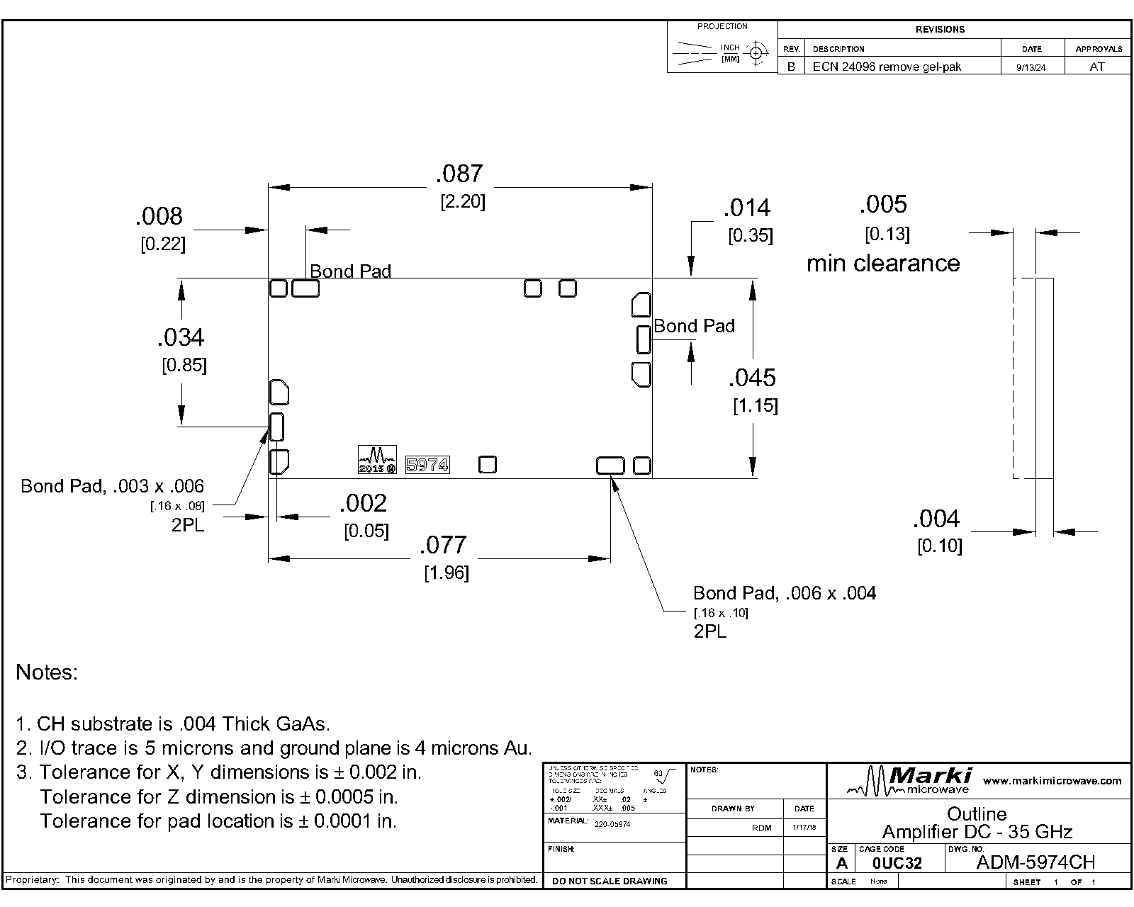
| Dimensions | - | 2.20x1.15mm |
ADM-5974CH
Broadband Distributed Amplifier
Specifications measured in a 50-Ohm system.
| Parameter | Test Conditions | Minimum Frequency (GHz) | Maximum Frequency (GHz) | Min | Typ | Max | Unit |
|---|---|---|---|---|---|---|---|
| Current Consumption | Vd: +5.0 to +7.0 Vg: -0.25 Volts | 0 | 35 | - | 150 | - | mA |
| Current Consumption | Vd: +5.0 to +7.0 Vg: 0 Volts | 0 | 35 | - | 220 | - | mA |
| Noise Figure | - | 0 | 35 | - | 6 | - | dB |
| Output IP3 | - | 0 | 35 | - | 27 | - | dBm |
| Output P1dB | - | 0 | 35 | - | 20 | - | dBm |
| Phase Noise @ 10 kHz Offset | - | 0 | 35 | - | -153 | - | dBc/Hz |
| Return Loss | - | 0 | 35 | - | 16 | - | dB |
| Saturated Output Power | With Negative Bias | 0 | 35 | - | 22 | - | dBm |
| Small Signal Gain | With Negative Bias | 0 | 35 | - | 14 | - | dB |
ADM-5974CH
Broadband Distributed Amplifier
+3, +7V Positive Bias, -0.25 Negative Bias


ADM-5974CH
Broadband Distributed Amplifier


ADM-5974CH
Broadband Distributed Amplifier


ADM-5974CH
Broadband Distributed Amplifier

ADM-5974CH
Broadband Distributed Amplifier