Port Diagram
Sales: 408-778-9952 | General: 408-778-4200 | Fax: 408-778-4300
Sales & Customer Support: [email protected]
Tech Support: [email protected]
The ADM-5931CH is a broadband, power-efficient, moisture-resistant GaAs PHEMT distributed amplifier chip. The ADM-5931CH is designed to provide optimal LO drive for T3 mixers. Typically, it provides 11 dB of gain and +18 dBm saturated output power while requiring only 85 mA of current. T3 linearity is enhanced by ADM-5931’s extended high frequency gain and lower even harmonic generation when compared to other distributed amplifiers in our catalog. It can be biased with internal circuitry, or with an external bias network for lower voltage and single supply operation. The enhanced moisture resistance process enables the bare chip to pass biased HAST testing without the use of a hermetically sealed package.

N/A
| Part Number | Description | Package | Green Status | Product Lifecycle | Export Classification |
|---|---|---|---|---|---|
| ADM-5931CH | Broadband Distributed Amplifier | CH | REACH RoHS | Released | EAR99 |
| Part Number | Description | Package | Green Status | Product Lifecycle | Export Classification |
|---|---|---|---|---|---|
| ADM-5931CH | Broadband Distributed Amplifier | CH | REACH RoHS | Released | EAR99 |
ADM-5931CH
Broadband Distributed Amplifier
| Revision Code | Revision Date | Comment |
|---|---|---|
| - | 2018-01-01 | Datasheet initial Release |
| A | 2019-07-01 | Thermal Resistance Spec Corrected |
| B | 2020-12-01 | Added Max Junction Temperature Specification |
ADM-5931CH
Broadband Distributed Amplifier
| Port | Function | Description | DC Equivalent Circuit |
|---|---|---|---|
| GND | Gnd | Back of chip should be connected to RF/DC ground with low electrical and thermal resistance. |  |
| RF In | RF Input | This pin is DC coupled and matched to 50 Ω. |  |
| Vd2 | Vd2 | Optional drain bias port. External decoupling capacitors are required. |  |
| Vd/RF Out | Vd / RF Out | This pad is DC coupled and matched to 50 Ω. | |
| Vg | Vg | Gate control for the amplifier. External decoupling capacitors are required. |  |
ADM-5931CH
Broadband Distributed Amplifier
| Parameter | Maximum Rating | Unit |
|---|---|---|
| Input Power | 20 | dBm |
| Maximum Operating Temperature | 85 | °C |
| Maximum Storage Temperature | 150 | °C |
| Max Junction Temperature to Maintain 10⁶ Hours Mean Time to Failure (MTTF): | 175 | °C |
| Minimum Operating Temperature | -55 | °C |
| Minimum Storage Temperature | -65 | °C |
| Negative Bias Current | 2 | mA |
| Negative Bias Voltage | -0.3 | V |
| Positive Bias Current | 150 | mA |
| Positive Bias Voltage | 9 | V |
| Power Dissipation | 2 | W |
| Thermal Resistance | 67 | ºC/W |
| Parameter | Details | Rating |
|---|---|---|
| ESD | < 250 Volts | HBM Class 0 |
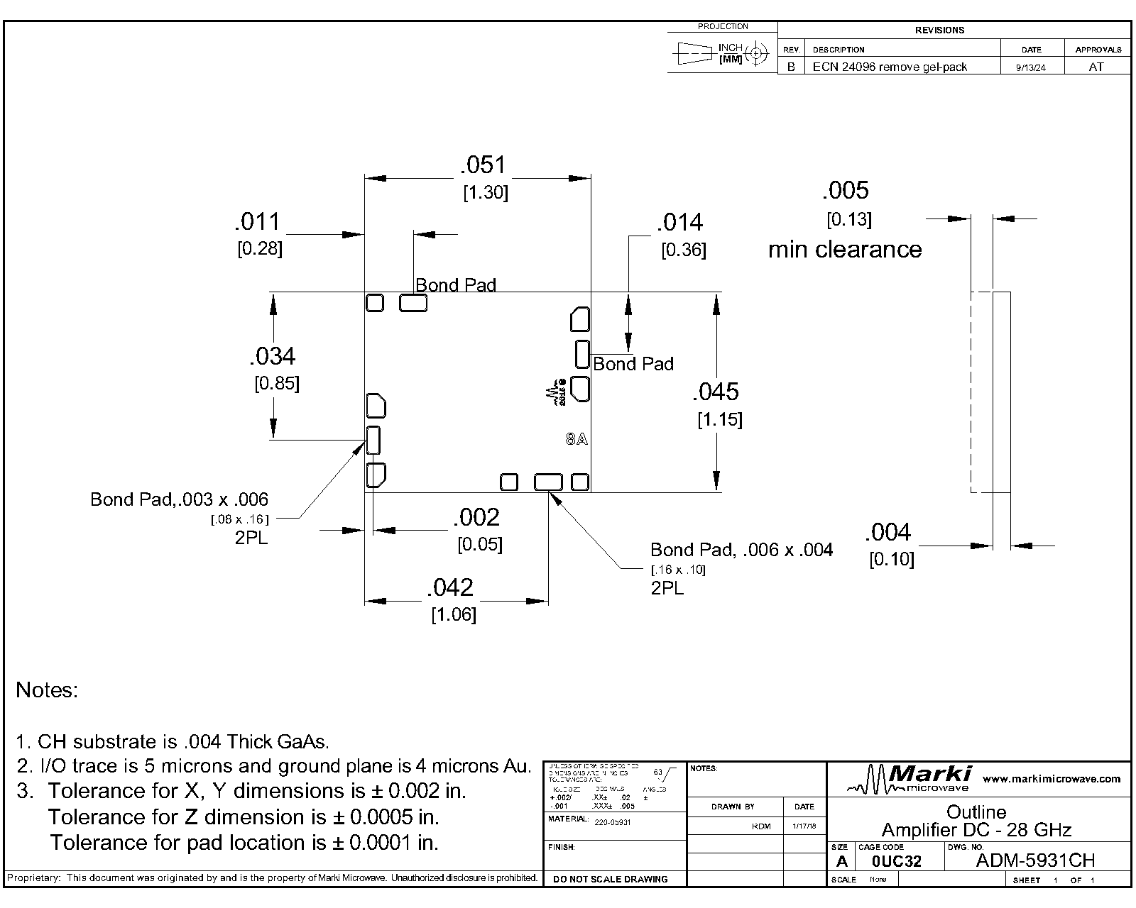
| Dimensions | - | 1.30 x 1.15 mm |
ADM-5931CH
Broadband Distributed Amplifier
Specifications measured in a 50-Ohm system.
| Parameter | Test Conditions | Minimum Frequency (GHz) | Maximum Frequency (GHz) | Min | Typ | Max | Unit |
|---|---|---|---|---|---|---|---|
| Current Consumption | Vd: +5.0 to +7.0 (External) Vg: -0.25 Volts | 0 | 28 | - | 85 | - | mA |
| Current Consumption | Vd: +5.0 to +7.0 (External) Vg: 0 Volts | 0 | 28 | - | 120 | - | mA |
| Input Power for Saturation | - | 0 | 28 | - | 8 | - | dBm |
| Input Return Loss | - | 0 | 28 | - | 16 | - | dB |
| Noise Figure | - | 0 | 28 | - | 6 | - | dB |
| Output IP3 | - | 0 | 28 | - | 27 | - | dBm |
| Output P1dB | - | 0 | 28 | - | 16 | - | dBm |
| Output Return Loss | - | 0 | 28 | - | 14 | - | dB |
| Phase Noise @ 10 kHz Offset | - | 0 | 28 | - | -153 | - | dBc/Hz |
| Saturated Output Power | With Negative Bias | 0 | 28 | - | 18 | - | dBm |
| Small Signal Gain | With Negative Bias | 0 | 28 | - | 11 | - | dB |
ADM-5931CH
Broadband Distributed Amplifier
Positive Only (+3, +7V) Bias (Bias tee on RF output), Grounded Gate (Bias tee on RF input)


ADM-5931CH
Broadband Distributed Amplifier


ADM-5931CH
Broadband Distributed Amplifier


ADM-5931CH
Broadband Distributed Amplifier

ADM-5931CH
Broadband Distributed Amplifier