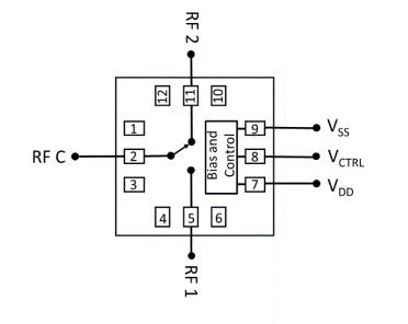
Port Diagram
A top-down x-ray view of the MSW2-1002HLGA package outline drawing is shown below.

Sales: 408-778-9952 | General: 408-778-4200 | Fax: 408-778-4300
Sales & Customer Support: [email protected]
Tech Support: [email protected]
The MSW2-1002HLGA is a reflective, single-pole double throw (SPDT) switch. The part is manufactured using a Silicon-On-Insulator (SOI) process. The switch operates from 100MHz to 20GHz with average insertion loss and isolation of 0.8 dB and 44 dB respectively and input power handling and hot switching capability of 33.5 dBm. The MSW2-1002HLGA requires positive and negative 3.3V supply inputs and is controlled via a single input pin compatible with LVTTL logic. This switch has a 50-Ohm characteristic impedance. The MSW2-1002HLGA is packaged in a compact 2.25x2.25 mm LGA for surface mount integration on circuit board-based systems.

| Part Number | Description | Package | Green Status | Product Lifecycle | Export Classification |
|---|---|---|---|---|---|
| MSW2-1002HLGA | 0.1-20 GHz Surface Mount High Power SPDT Switch | LGA | REACH RoHS | Released | EAR99 |
| EVB-MSW2-1002H | 0.1 - 20 GHz Surface Mount SPDT Switch | EVB | REACH RoHS | Released | EAR99 |
MSW2-1002HLGA
0.1-20 GHz Surface Mount High Power SPDT Switch
| Revision Code | Revision Date | Comment |
|---|---|---|
| - | 2024-05-21 | Initial Release |
MSW2-1002HLGA
0.1-20 GHz Surface Mount High Power SPDT Switch
A top-down x-ray view of the MSW2-1002HLGA package outline drawing is shown below.
MSW2-1002HLGA
0.1-20 GHz Surface Mount High Power SPDT Switch
| Port | Function | Description | DC Equivalent Circuit |
|---|---|---|---|
| 11 | RF2 | RF port 2 of the device, impedance looking into this port matches RFC load impedance in the ON state. This port is reflective and shorted to GND in the OFF state. This port is DC coupled. A DC blocking capacitor is required ONLY if max DC voltages will be exceeded. | - |
| 1,3,4,6,10,12 | Ground | These pins should be connected to RF/DC ground. All GND pins are internally connected. | - |
| 2 | RFC | RF common port of the device. This port is DC coupled. A DC blocking capacitor is required ONLY if max DC voltages will be exceeded. This port has a 50 Ohm input impedance when the active port is terminated with a 50 Ohm load. | - |
| 5 | RF1 | RF port 1 of the device, impedance looking into this port matches RFC load impedance in the ON state. This port is reflective and shorted to GND in the OFF state. This port is DC coupled. A DC blocking capacitor is required ONLY if max DC voltages will be exceeded. | - |
| 7 | VDD | Positive DC supply pin. (+3.3V). Port has an ESD clamp to GND. | - |
| 8 | VCTRL | Control voltage input pin. Low Voltage Transistor-Transistor Logic (LVTTL) compatible. Port has ESD clamp to GND and VDD. An external pull-down resistor is recommended on this pin. | - |
| 9 | VSS | Negative DC supply pin. (-3.3V). Port has an ESD clamp to GND. | - |
| Paddle | Ground | IC backside must be connected to a DC/RF ground with high thermal and electrical conductivity. | - |
MSW2-1002HLGA
0.1-20 GHz Surface Mount High Power SPDT Switch
The Absolute Maximum Ratings indicate limits beyond which damage may occur to the device. If these limits are exceeded, the device may become inoperable or have a reduced lifetime.
| Parameter | Maximum Rating | Unit |
|---|---|---|
| Control Voltage | 3.9 | V |
| Max Current on any RF Port, Unbiased | 50 | μA |
| Max DC on any RF Port, Unbiased | 0.5 | V |
| Max Hot Switching RF Input Power | 33.5 | dBm |
| Maximum Operating Temperature for MTTF > 1E6 hours | 105 | °C |
| Maximum Storage Temperature | 150 | °C |
| Max Junction Temperature for MTTF of > 1E6 hours | 135 | °C |
| Max Power Dissipation for MTTF of > 1E6 hours at 85°C Baseplate Temperature | 0 | mW |
| Minimum Operating Temperature | -40 | °C |
| Minimum Storage Temperature | -60 | °C |
| Negative Supply Voltage | -3.6 | V |
| Positive Supply Voltage | 3.6 | V |
| RF Input Power, Nominal Bias | 33.5 | dBm |
| RF Input Power, Unbiased | 21 | dBm |
| θJC, Junction to Ambient Thermal Resistance | 0 | ºC/W |
| Parameter | Details | Rating |
|---|---|---|
| ESD | 250 to < 500 Volts | HBM Class 1A |
| Dimensions | - | 2.25 x 2.25 mm |
| Moisture Sensitivity Level | - | MSL 3 |
The Recommended Operating Conditions indicate the limits, inside which the device should be operated, to guarantee the performance given in Electrical Specifications. Operating outside these limits may not necessarily cause damage to the device, but the performance may degrade outside the limits of the electrical specifications. For limits, above which damage may occur, see Absolute Maximum Ratings.
| Parameter | Min | Nominal | Max | Unit |
|---|---|---|---|---|
| Control Voltage Low, VINL | 0 | - | 1.55 | V |
| Negative DC Voltage | -3.45 | -3.3 | -3.15 | V |
| Control Current, IINL | - | - | 1 | μA |
| Ta Ambient Temperature | -40 | 25 | 101 | °C |
| Control Voltage High, VINH | 1.63 | - | 3.45 | V |
| Positive DC Voltage | 3.15 | 3.3 | 3.45 | V |
| Control Current, IINH | - | - | 1 | μA |
| Negative Supply Current | - | 550 | - | μA |
| Positive Supply Current | - | 650 | - | μA |
MSW2-1002HLGA
0.1-20 GHz Surface Mount High Power SPDT Switch
The electrical specifications apply at TA=+25 °C in a 50 Ω system. Unless otherwise noted, all specifications are for VDD=3.3V, VSS=-3.3V and VCTRL = 0 or 3.3V (both switch paths) with all ports terminated into 50 Ω loads.
| Parameter | Test Conditions | Minimum Frequency (GHz) | Maximum Frequency (GHz) | Min | Typ | Max | Unit |
|---|---|---|---|---|---|---|---|
| Input IP3 | Two Tones @ +12dBm, dF = 1 MHz | 0.1 | 20 | - | 54 | - | dBm |
| Input P1dB | Vdd=3.3V, Vss=-3.3V, Vctrl = 0 or 3.3V | 0.1 | 20 | - | 33.5 | - | dBm |
| Insertion Loss | Vdd=3.3V, Vss=-3.3V, Vctrl = 0 or 3.3V | 0.1 | 20 | - | 0.8 | - | dB |
| Isolation | Vdd=3.3V, Vss=-3.3V, Vctrl = 0 or 3.3V | 0.1 | 20 | - | 44 | - | dB |
| Isolation, RFC to any non-active Port | Vdd=3.3V, Vss=-3.3V, Vctrl = 0 or 3.3V | 0.1 | 20 | - | 41 | - | dB |
| Make-before-break overlap | - | 0.1 | 20 | - | 42 | - | ns |
| Nominal RF Impedance | Vdd = 3.3V. Vss = -3.3V, Vctrl = 0 or 3.3V | - | - | - | 50 | - | Ω |
| Off-Time | 50% VCTRL to 90% RF output | 0.1 | 20 | - | 67 | - | ns |
| On-Time | 50% VCTRL to 90% RF output | 0.1 | 20 | - | 67 | - | ns |
| Return Loss | Vdd=3.3V, Vss=-3.3V, Vctrl = 0 or 3.3V | 0.1 | 20 | - | 21 | - | dB |
| RF Settling Time | 50% VCTRL to 0.05dB final RF output | 0.1 | 20 | - | 104 | - | ns |
| RF Settling Time | 50% VCTRL to 0.1dB final RF output | 0.1 | 20 | - | 99 | - | ns |
| Risetime/Falltime | 10-90% of RF output | 0.1 | 20 | - | 4 | - | ns |
| VCTRL Latency | 50% VCTRL to start of RF state transition | 0.1 | 20 | - | 58 | - | ns |
MSW2-1002HLGA
0.1-20 GHz Surface Mount High Power SPDT Switch


MSW2-1002HLGA
0.1-20 GHz Surface Mount High Power SPDT Switch
Download : Outline 2D Drawing
Notes (unless otherwise specified):
MSW2-1002HLGA
0.1-20 GHz Surface Mount High Power SPDT Switch
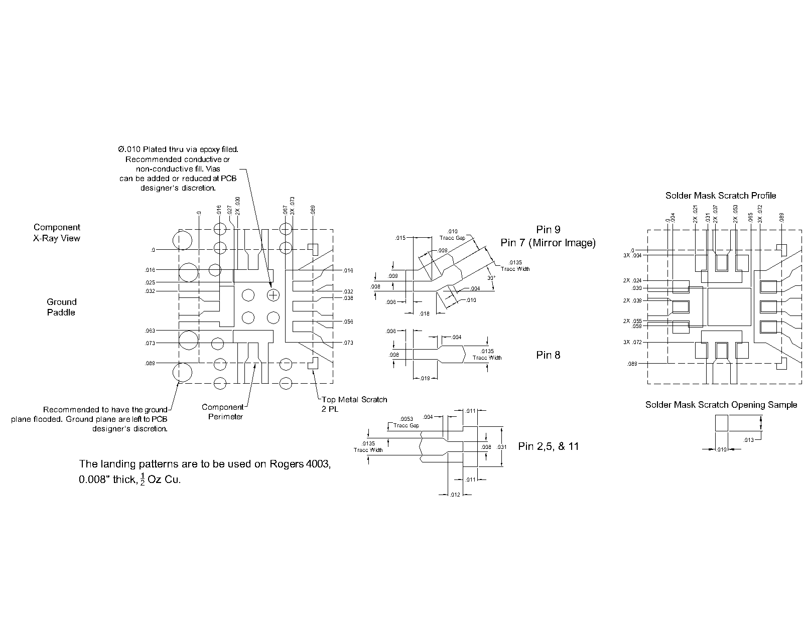
Download : Footprint Drawing
MSW2-1002HLGA
0.1-20 GHz Surface Mount High Power SPDT Switch
