Port Diagram
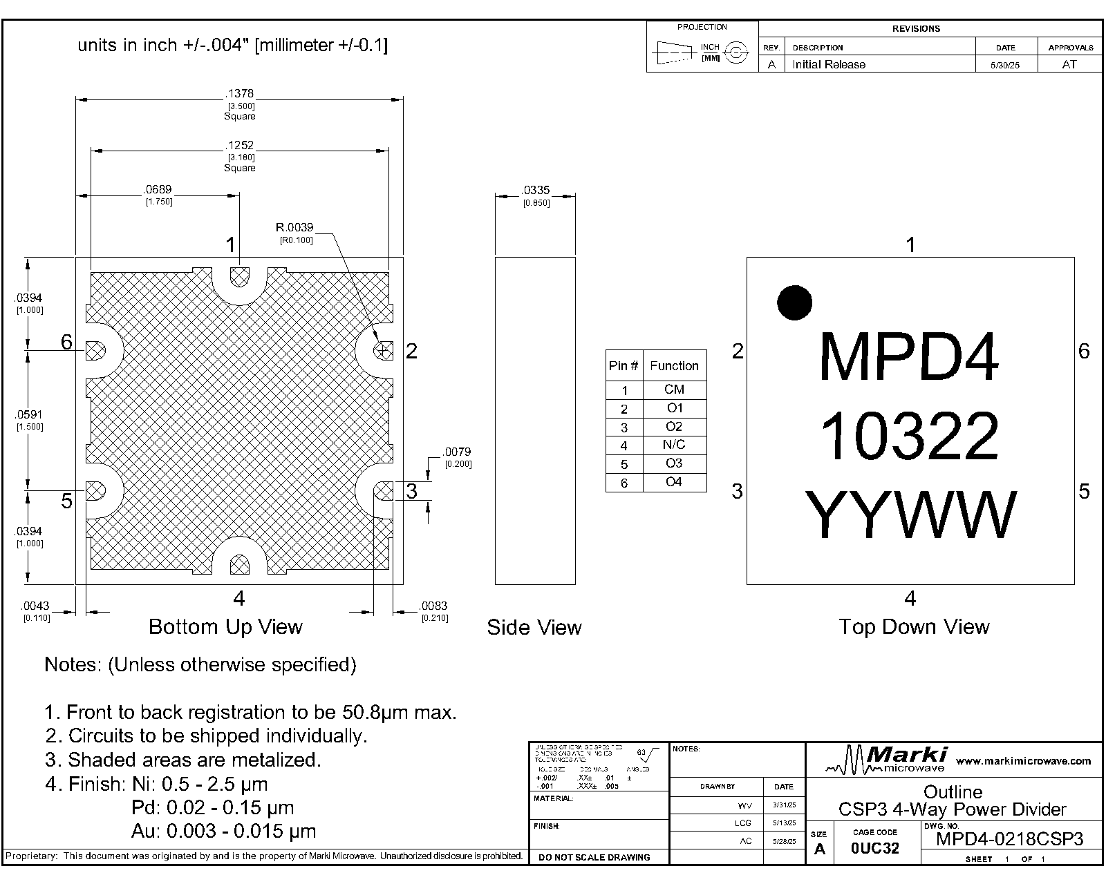
A top-down view of the MPD4-0218CSP3 package outline drawing is shown below. The MMIC Power dividers are passive reciprocal devices allowing either power splitting or power combining.
Sales: 408-778-9952 | General: 408-778-4200 | Fax: 408-778-4300
Sales & Customer Support: [email protected]
Tech Support: [email protected]
The MPD4-0218CSP3 is a small footprint MMIC 2-18 GHz 4-Way power divider/power splitter featuring high 29 dB isolation and low 0.8 dB excess insertion loss in our compact CSP3 chip scale package. It is much smaller than a printed PCB Wilkinson Power Divider/Combiner. It can be used as an equal amplitude/phase power splitter or a power combiner with excellent isolation. Tight fabrication tolerances result in less unit-to-unit variation than traditional power divider technologies, allowing for accurate simulations using the provided S5P file taken from measured production units. The 3.5 mm CSP3 package enables extreme miniaturization of SMT footprint making the MPD4-0218CSP3 ideal for applications prioritizing low SWaP.


| Part Number | Description | Package | Green Status | Product Lifecycle | Export Classification |
|---|---|---|---|---|---|
| MPD4-0218CSP3 | 2-18 GHz MMIC 4-Way Wilkinson Power Divider/Power Splitter | CSP3 | REACH RoHS | Released | EAR99 |
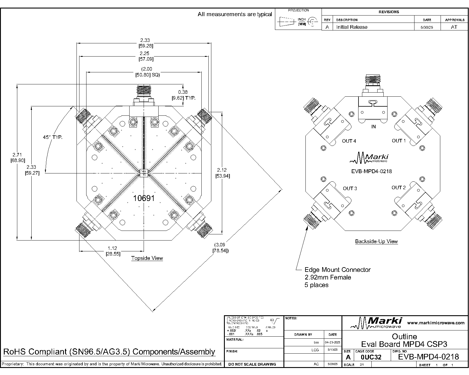
| EVB-MPD4-0218 | Evaluation Board, 2 - 18 GHz MMIC 4-Way Wilkinson Power Divider/Power Splitter | EVB | RoHS REACH | Released | EAR99 |
| Part Number | Description | Package | Green Status | Product Lifecycle | Export Classification |
|---|---|---|---|---|---|
| MPD4-0218CSP3 | 2-18 GHz MMIC 4-Way Wilkinson Power Divider/Power Splitter | CSP3 | REACH RoHS | Released | EAR99 |
| EVB-MPD4-0218 | Evaluation Board, 2 - 18 GHz MMIC 4-Way Wilkinson Power Divider/Power Splitter | EVB | RoHS REACH | Released | EAR99 |
MPD4-0218CSP3
2-18 GHz MMIC 4-Way Wilkinson Power Divider/Power Splitter
| Revision Code | Revision Date | Comment |
|---|---|---|
| - | 2025-07-09 | Initial Release |
| A | 2025-08-27 | Port Functions Description Updated |
| B | 2025-11-17 | Power Handling Updated |
MPD4-0218CSP3
2-18 GHz MMIC 4-Way Wilkinson Power Divider/Power Splitter
A top-down view of the MPD4-0218CSP3 package outline drawing is shown below. The MMIC Power dividers are passive reciprocal devices allowing either power splitting or power combining.
MPD4-0218CSP3
2-18 GHz MMIC 4-Way Wilkinson Power Divider/Power Splitter
| Port | Function | Description | DC Equivalent Circuit |
|---|---|---|---|
| Ground Paddle | Gnd | Ground paddle should be connected to RF ground |  |
| Pin 1 | Common | Pin 1 is the common input/output pin. It is DC open to the other 4 pins and open to ground. |  |
| Pin 2 | Input/Output 1 | Pin 2 is an input/output pin. It is DC short to the other 4 pins and open to ground. | |
| Pin 3 | Input/Output 2 | Pin 3 is an input/output pin. It is DC short to the other 4 pins and open to ground. | |
| Pin 4 | NC | Pin 4 is not internally connected. It can be connected to ground for normal operation. |  |
| Pin 5 | Input/Output 3 | Pin 5 is an input/output pin. It is DC short to the other 4 pins and open to ground. | |
| Pin 6 | Input/Output 4 | Pin 6 is an input/output pin. It is DC short to the other 4 pins and open to ground. | |
MPD4-0218CSP3
2-18 GHz MMIC 4-Way Wilkinson Power Divider/Power Splitter
The Absolute Maximum Ratings indicate limits beyond which damage may occur to the device. If these limits are exceeded, the device may be inoperable or have a reduced lifetime.
| Parameter | Maximum Rating | Unit |
|---|---|---|
| DC Current | 40 | mA |
| Maximum Operating Temperature | 100 | °C |
| Maximum Storage Temperature | 125 | °C |
| Minimum Operating Temperature | -55 | °C |
| Minimum Storage Temperature | -65 | °C |
| RF Power Handling as a Power Combiner 1 | 1 | W |
| RF Power Handling as a Power Divider 2 | 10 | W |
[1] Power handling as a combiner is specified per port with all other ports terminated. Under worst-case odd-mode conditions, adjacent port pairs (Pins 2–3 and Pins 5–6) must not experience differential signals exceeding 1 W.
[2] Measured with a 6 GHz CW
| Parameter | Details | Rating |
|---|---|---|
| ESD | 250 to < 500 Volts | HBM Class 1A |
| Dimensions | - | 3.50 x 3.50 mm |
| Moisture Sensitivity Level | - | MSL 1 |
MPD4-0218CSP3
2-18 GHz MMIC 4-Way Wilkinson Power Divider/Power Splitter
The electrical specifications apply at TA=+25°C in a 50Ω system. Min and Max limits are guaranteed at TA=+25°C.
| Parameter | Test Conditions | Minimum Frequency (GHz) | Maximum Frequency (GHz) | Min | Typ | Max | Unit |
|---|---|---|---|---|---|---|---|
| Amplitude Balance | Adjacent Ports | 2 | 18 | - | 0.16 | - | dB |
| Amplitude Balance | Non-Adjacent Ports | 2 | 18 | - | 0.15 | - | dB |
| Common Port Return Loss | - | 2 | 18 | - | 22 | - | dB |
| Excess Insertion Loss 1 | - | 2 | 18 | - | 0.8 | - | dB |
| Impedance | - | 2 | 18 | - | 50 | - | Ω |
| Isolation | Adjacent Ports | 2 | 18 | - | 22 | - | dB |
| Isolation | Non-Adjacent Ports | 2 | 18 | - | 29 | - | dB |
| Nominal Phase Shift | - | 2 | 18 | - | 0 | - | ° |
| Nominal Power Splitting | - | 2 | 18 | - | 6 | - | dB |
| Output Return Loss | - | 2 | 18 | - | 21 | - | dB |
| Phase Balance | Adjacent Ports | 2 | 18 | - | 2.2 | - | ° |
| Phase Balance | Non-Adjacent Ports | 2 | 18 | - | 2.8 | - | ° |
[1] Excess Insertion Loss is loss in addition to power splitting loss, calculated as (Common Port to Output Port Insertion Loss) – (Power splitting loss of 6 dB)
MPD4-0218CSP3
2-18 GHz MMIC 4-Way Wilkinson Power Divider/Power Splitter


MPD4-0218CSP3
2-18 GHz MMIC 4-Way Wilkinson Power Divider/Power Splitter


Measured data is de-embedded from fixture using automatic fixture removal (AFR).
MPD4-0218CSP3
2-18 GHz MMIC 4-Way Wilkinson Power Divider/Power Splitter
MPD4-0218CSP3
2-18 GHz MMIC 4-Way Wilkinson Power Divider/Power Splitter
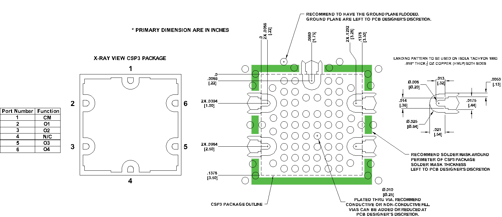
Download : Footprint Drawing
MPD4-0218CSP3
2-18 GHz MMIC 4-Way Wilkinson Power Divider/Power Splitter