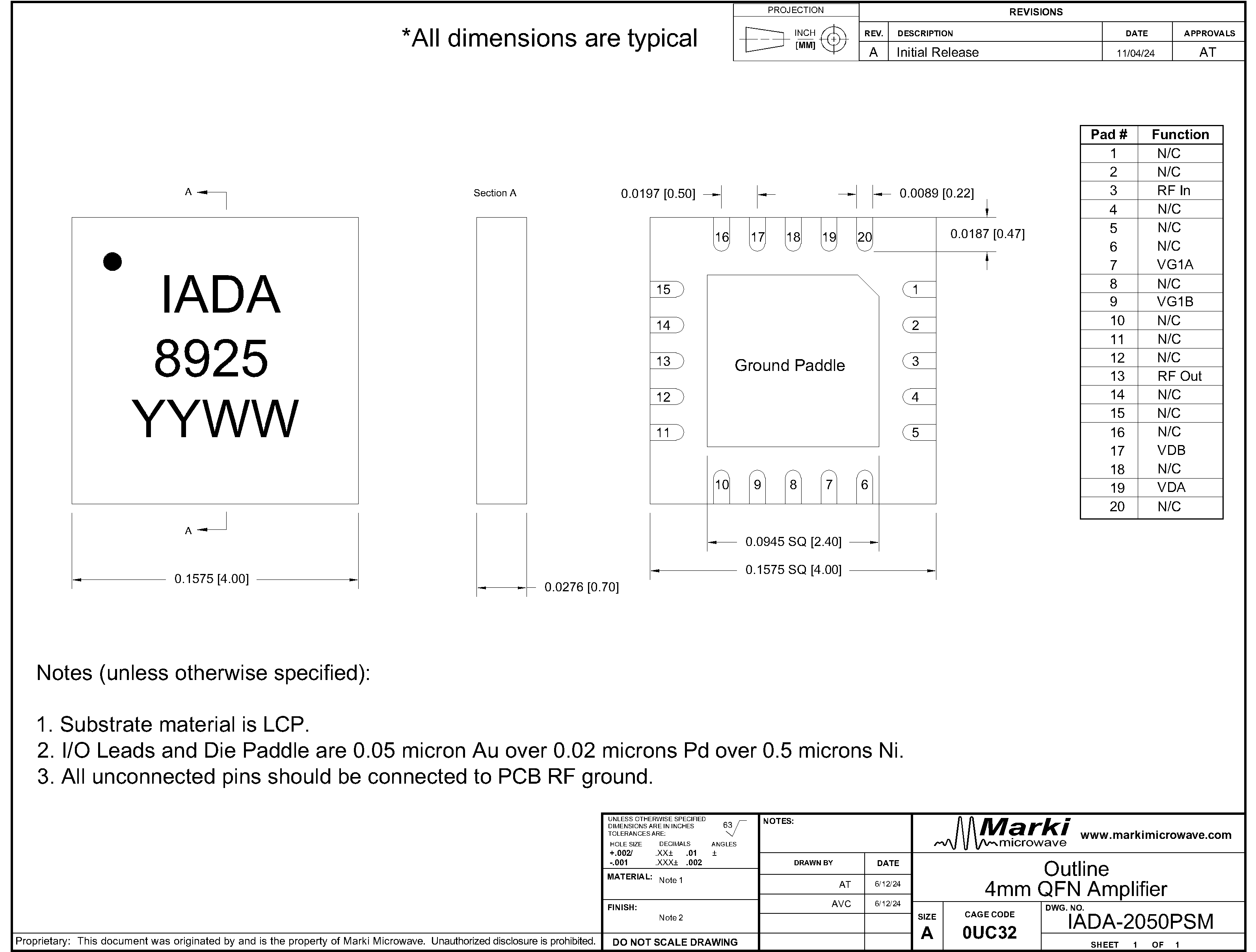
Port Diagram
A top-down x-ray view of the IADA-2050PSM is shown below.

Sales: 408-778-9952 | General: 408-778-4200 | Fax: 408-778-4300
Sales & Customer Support: [email protected]
Tech Support: [email protected]
The IADA-2050PSM is an integrated MMIC active doubler fabricated with GaAs Schottky diodes. This operates over a guaranteed 10 to 25 GHz input frequency range or a doubled output frequency range of 20to 50 GHz. It features excellent conversion loss, superior isolations and harmonic suppressions across a broad bandwidth.

| Part Number | Description | Package | Green Status | Product Lifecycle | Export Classification |
|---|---|---|---|---|---|
| IADA-2050PSM | Amplifier/Doubler/Amplifier | PSM | REACH RoHS | Released | EAR99 |
| EVB-IADA-2050P | Evaluation Board, 20-50GHz Amplified Doubler | EVB | REACH RoHS | Released | EAR99 |
IADA-2050PSM
Amplifier/Doubler/Amplifier
| Revision Code | Revision Date | Comment |
|---|---|---|
| - | 2024-08-26 | Initial Release |
| A | 2026-03-02 | Added Input vs. Output Power Plots over Temperature |
| B | 2026-06-18 | Added Thermal Resistance Rating |
IADA-2050PSM
Amplifier/Doubler/Amplifier
A top-down x-ray view of the IADA-2050PSM is shown below.
IADA-2050PSM
Amplifier/Doubler/Amplifier
| Port | Function | Description | DC Equivalent Circuit |
|---|---|---|---|
| Paddle | Ground | Ground pad should be connected to RF/DC ground with high electrical and thermal conductivity. |  |
| Pin 13 | Output | This pin is internally DC blocked and matched to 50 Ω at frequency range 20 – 50 GHz. |  |
| Pin 17 | VDB | Drain bias for the output amplifier. This pin must be connected to a positive power supply. Set this voltage to +5V for normal operation. |  |
| Pin 19 | VDA | Drain bias for the input amplifier. This pin must be connected to a positive power supply. Set this voltage to +5V for normal operation. | |
| Pin 3 | Input | This pin is internally DC blocked and matched to 50 Ω at frequency range 10 - 25 GHz. | |
| Pin 7 | VG1A | Gate control for the input amplifier. This pad must be connected to a negative power supply. Set this voltage to -0.15V for normal operation. |  |
| Pin 9 | VG1B | Gate control for the output amplifier. This pad must be connected to a negative power supply. Set this voltage to -0.15V for normal operation. | |
IADA-2050PSM
Amplifier/Doubler/Amplifier
The Absolute Maximum Ratings indicate limits beyond which damage may occur to the device. If these limits are exceeded, the device may be inoperable or have a reduced lifetime.
| Parameter | Maximum Rating | Unit |
|---|---|---|
| Maximum Operating Temperature | 85 | °C |
| Maximum Storage Temperature | 150 | °C |
| Minimum Operating Temperature | -55 | °C |
| Minimum Storage Temperature | -65 | °C |
| Negative Bias Current | 2 | mA |
| Negative Bias Voltage | -2 | V |
| Positive Bias Current | 550 | mA |
| Positive Bias Voltage | 5.5 | V |
| Power Dissipation | 2.5 | W |
| RF Input Power | 10 | dBm |
| Thermal Resistance, θJC | 27 | ºC/W |
| Parameter | Details | Rating |
|---|---|---|
| ESD | < 250 Volts | HBM Class 0 |
| Dimensions | - | 4 x 4 mm |
| Moisture Sensitivity Level | - | MSL 1 |
| Parameter | Min | Nominal | Max | Unit |
|---|---|---|---|---|
| Gate Bias DC Voltage (Vg) | - | -0.15 | - | V |
| Positive DC Voltage (Vd) | - | 5 | - | V |
| Input Power | - | 5 | - | - |
IADA-2050PSM
Amplifier/Doubler/Amplifier
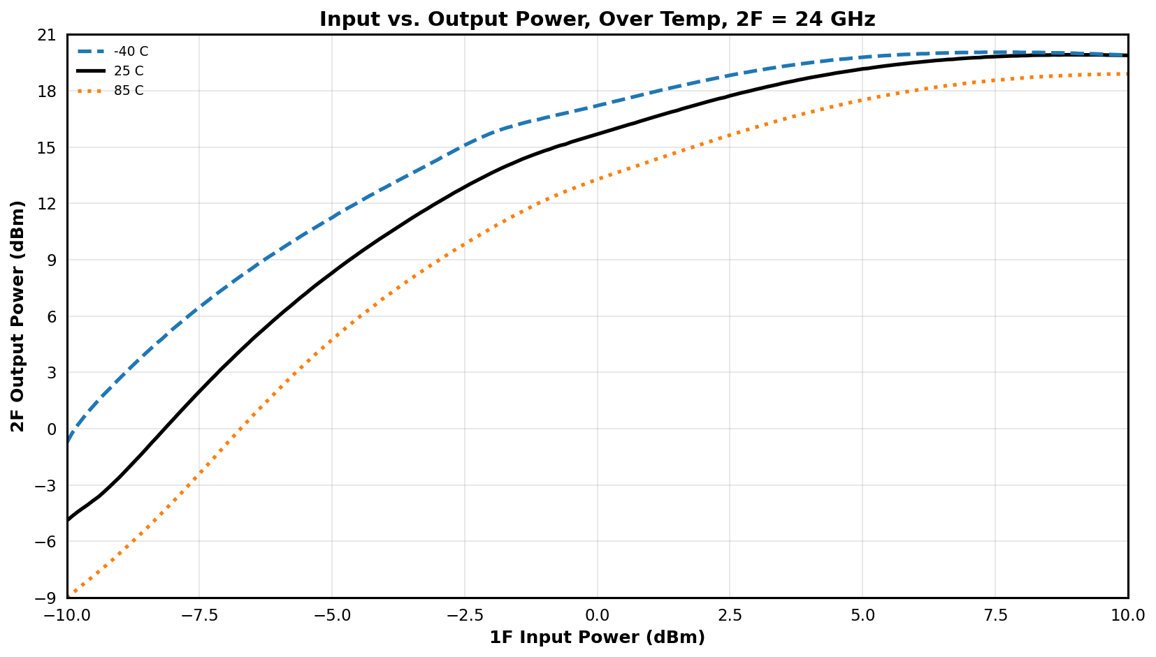
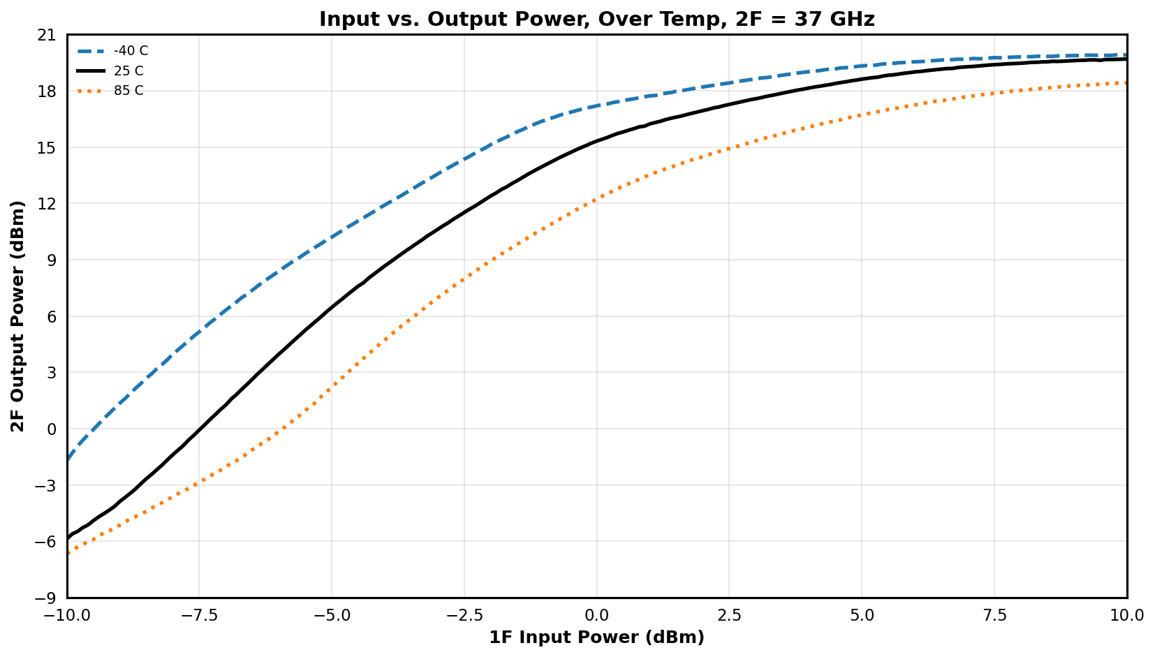
The electrical specifications apply at TA=+25°C in a 50Ω system. Suppression is relative to doubled output power.
| Parameter | Test Conditions | Minimum Frequency (GHz) | Maximum Frequency (GHz) | Min | Typ | Max | Unit |
|---|---|---|---|---|---|---|---|
| Input Return Loss | Vd = 5V, Vg = -0.15V | 10 | 25 | - | 15 | - | dB |
| Output Return Loss | Vd = 5V, Vg = -0.15V | 20 | 50 | - | 15 | - | dB |
| Suppression, 1F | Pin = +5dBm | 10 | 25 | - | 25 | - | dBc |
| Suppression, 3F | Pin = +5dBm | 30 | 67 | - | 35 | - | dBc |
| Suppression, 4F | Pin = +5dBm | 40 | 67 | - | 18 | - | dBc |
| Current Consumption 1 | Vd = 5V, Vg = -0.15V | - | - | - | 233 | - | mA |
| Input Frequency Range | - | - | - | 10 | - | 25 | GHz |
| Input Power | Input = 10 - 25 GHz | - | - | - | 5 | - | dBm |
| Output Converted Power, 2F (out) | Output Freq = 20.0 - 50.0 GHz, Pin = +5dBm | - | - | - | 17 | - | dBm |
| Output Frequency Range | - | - | - | 20 | - | 50 | GHz |
[1] It is required that the negative bias be applied before or concurrent with the positive bias.
IADA-2050PSM
Amplifier/Doubler/Amplifier
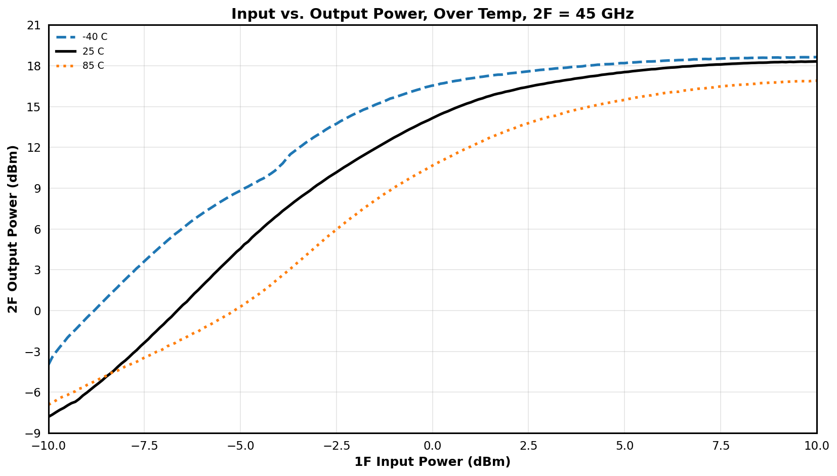
Unless otherwise specified, the performance plots below are measured with +5dBm input power.


IADA-2050PSM
Amplifier/Doubler/Amplifier
IADA-2050PSM
Amplifier/Doubler/Amplifier

IADA-2050PSM
Amplifier/Doubler/Amplifier
IADA-2050PSM
Amplifier/Doubler/Amplifier
Download : Footprint Drawing

IADA-2050PSM
Amplifier/Doubler/Amplifier