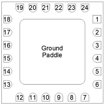
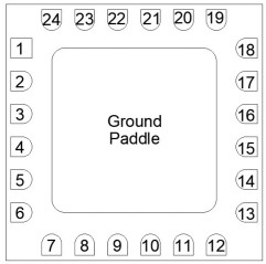
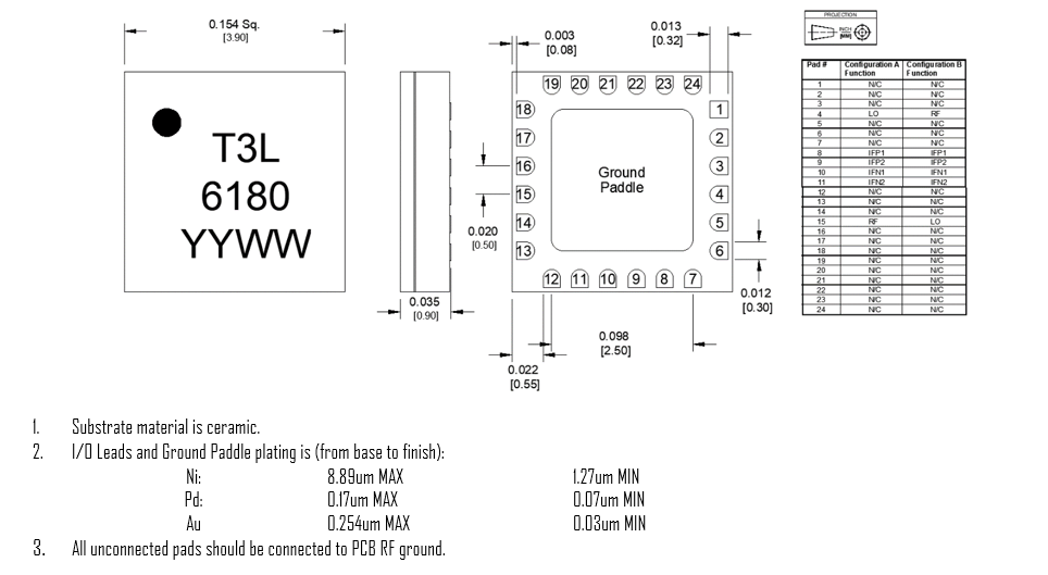
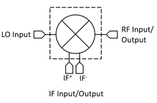
Device Overview

General Description

MT3D-0113LSM is a GaAs MMIC triple balanced mixer with high dynamic range and low conversion loss. This mixer belongs to the T3 family which offers high IP3, P1dB, and broad operating bandwidths for applications in the S, C and X bands. The MT3D-0113LSM has on-chip baluns for the LO and RF ports, while offering differential ports on the IF for flexible operation with an external balun or differential interface. The MT3D-0113LSM is available in a 4x4 mm¬2 QFN package.

Photo of MT3D-0113LSM-2

Features

  • High LO to RF isolation
  • Broad, overlapping RF/LO & IF bands
  • Differential IF ports

Applications

  • Test and Measurement Equipment
  • S/C/X band radar

Functional Block Diagram

Block Diagram

Part Ordering Options

Part NumberDescriptionPackageGreen StatusProduct LifecycleExport Classification
MT3D-0113LSM-2GaAs MMIC T3 Mixer with Differential IFQFN

REACH

RoHS

ReleasedEAR99

Table Of Contents

Revision History

Revision CodeRevision DateComment
-2021-08-01Datasheet Initial Release
A2022-10-01Spurs, Harmonic Isolations, and EVB part number added.

Rev: A | Copyright © 2021 - 2022 Marki Microwave LLC.

2

Port Configuration and Functions

Port Diagram

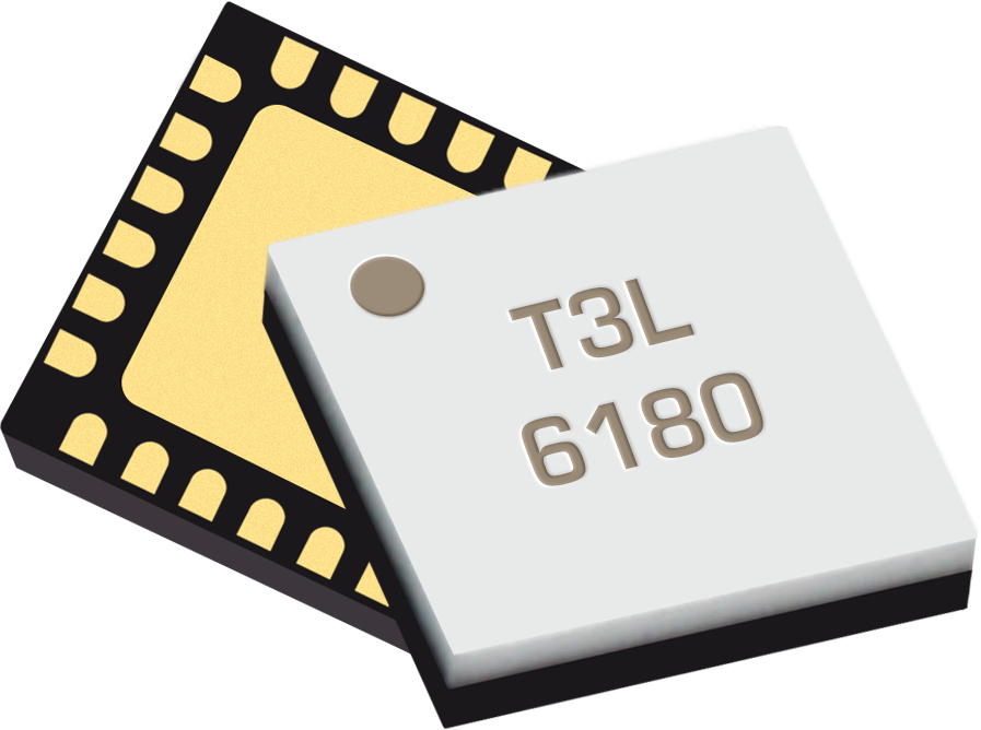
A bottom-up view of the MT3D-0113LSM’s SM package outline drawing is shown below. The MT3D-0113LSM has the input and output ports given in Port Functions. The MT3D-0113LSM can be used in either an up or down conversion. Configuration A/B refer to the same part number (MT3D-0113LSM) used in one of two different ways for optimal spurious performance. For configuration A, input the LO into pin 4, use pin 15 for the RF. For configuration B, input the LO into pin 4, use pin 15 for the RF. Refer to section 4.1 for explanation of Configuration A and B operation.

Diagram of the port configuration for MT3D-0113LSM-2

Port Functions

Configuration A

PortFunctionDescriptionDC Equivalent
Circuit
GNDGround SM package ground path is provided through the ground paddle.Equivalent circuit for the Ground
Pin 10 and 11IF N1 and N2 Pins 10 and 11 are DC coupled to the diodes. Blocking capacitors are required. Pins 8 and 9 should be DC blocked and connected prior to balun.Equivalent circuit for the IF N1 and N2
Pin 15RF Pin 15 is DC short for the SM package.Equivalent circuit for the RF
Pin 4LO Pin 4 is DC short for the SM package.Equivalent circuit for the LO
Pin 8 and 9IF P1 and P2 Pins 8 and 9 are DC coupled to the diodes. Blocking capacitors are required. Pins 8 and 9 should be DC blocked and connected prior to balun.Equivalent circuit for the IF P1 and P2

Rev: A | Copyright © 2021 - 2022 Marki Microwave LLC.

3

Configuration B

PortFunctionDescriptionDC Equivalent
Circuit
GNDGround SM package ground path is provided through the ground paddle.Equivalent circuit for the Ground
Pin 10 and 11IF N1 and N2 Pins 10 and 11 are DC coupled to the diodes. Blocking capacitors are required. Pins 8 and 9 should be DC blocked and connected prior to balun.Equivalent circuit for the IF N1 and N2
Pin 15LO Pin 15 is DC short for the SM package.Equivalent circuit for the LO
Pin 4RF Pin 4 is DC short for the SM package.Equivalent circuit for the RF
Pin 8 and 9IF P1 and P2 Pins 8 and 9 are DC coupled to the diodes. Blocking capacitors are required. Pins 8 and 9 should be DC blocked and connected prior to balun.Equivalent circuit for the IF P1 and P2

Rev: A | Copyright © 2021 - 2022 Marki Microwave LLC.

4

Specifications

Absolute Maximum Ratings

The Absolute Maximum Ratings indicate limits beyond which damage may occur to the device. If these limits are exceeded, the device may be inoperable or have a reduced lifetime.

ParameterMaximum RatingUnit
Maximum Operating Temperature 100°C
Minimum Operating Temperature -40°C
Minimum Storage Temperature 125°C
Minimum Storage Temperature -40°C
Pin 8, 9, 10, 11 DC Current 0mA
Power Handling, at any Port 30dBm

Package Information

ParameterDetailsRating
ESD250 to < 500 VoltsHBM Class 1A
Dimensions-4 x 4 mm
Moisture Sensitivity Level-MSL 1

The Recommended Operating Conditions indicate the limits, inside which the device should be operated, to guarantee the performance given in Electrical Specifications Operating outside these limits may not necessarily cause damage to the device, but the performance may degrade outside the limits of the electrical specifications. For limits, above which damage may occur, see Absolute Maximum Ratings.

ParameterMinNominalMaxUnit
Ambient Temperature -4025100°C
LO Input Power 111725dBm

Rev: A | Copyright © 2021 - 2022 Marki Microwave LLC.

5

Electrical Specifications

The electrical specifications apply at TA=+25°C in a 50Ω system. Typical data shown is for the connectorized EVAL package mixer† used with a +17 dBm sine wave LO. Typical IP3 data shown for a +19 dBm square wave LO. Min and Max limits apply only to our connectorized units and are guaranteed at TA=+25°C.

ParameterPort ConfigurationTest ConditionsMinTypMaxUnit
Conversion Loss 1ARF/LO = 1.5 - 13 GHz
I = 91 MHz
-7.5-dB
Input IP3 2ARF/LO = 1.5 - 13 GHz
I = 91 MHz
-27-dBm
LO-IF Isolation AIF/LO = 1.5 - 13 GHz
-43-dB
LO-RF Isolation ARF/LO = 1.5 - 13 GHz
-43-dB
Noise Figure 3ARF/LO = 1.5 - 13 GHz
I = 91 MHz
-7.5-dB
RF-IF Isolation ARF/IF = 1.5 - 13 GHz
-42-dB
Conversion Loss 4BRF/LO = 1.5 - 13 GHz
I = 91 MHz
-7.5-dB
Input IP3 5BRF/LO = 1.5 - 13 GHz
I = 91 MHz
-27-dBm
LO-IF Isolation BIF/LO = 1.5 - 13 GHz
-42-dB
LO-RF Isolation BRF/LO = 1.5 - 13 GHz
-37-dB
Noise Figure 6BRF/LO = 1.5 - 13 GHz
I = 91 MHz
-7.5-dB
RF-IF Isolation BRF/IF = 1.5 - 13 GHz
-43-dB
IF Frequency Range 7-----GHz
LO Frequency Range --1.5-13GHz
RF Frequency Range --1.5-13GHz

[1][4] Measured as a down converter to a fixed 91 MHz IF. Unless otherwise stated, frequency conversion done using a highside LO.

[2][5] IP3 depends on LO drive condition. Reported table value is measured with a square wave LO formed using 2x ADM1-0026PA in series with +10 dBm input into the first stage. LO Power reported in plots is of the fundamental tone only. Square wave LO power in plots is stepped down using broadband DC-40 GHz attenuators.

[3][6] Mixer Noise Figure typically measures within 0.5 dB of conversion loss for IF frequencies greater than 5 MHz.

[7] IF range max value is determined by off-chip balun. Contact [email protected] for details.

Rev: A | Copyright © 2021 - 2022 Marki Microwave LLC.

6

Typical Performance Plots

Conversion Loss: 91 MHz IF, Highside LO (dB) graph for MT3D-0113LSM-2
Configuration A Conversion Loss vs. LO Power: 100 MHz IF (dB) graph for MT3D-0113LSM-2
Configuration B Conversion Loss vs. LO Power: 100 MHz IF (dB) graph for MT3D-0113LSM-2
LO to RF Isolation (dB) graph for MT3D-0113LSM-2
LO to IF Isolation (dB) graph for MT3D-0113LSM-2

Rev: A | Copyright © 2021 - 2022 Marki Microwave LLC.

7

RF to IF Isolation (dB) graph for MT3D-0113LSM-2
RF Return Loss (dB) graph for MT3D-0113LSM-2
LO Return Loss (dB) graph for MT3D-0113LSM-2
Input 1 dB Compression vs LO Power: 5 GHz RF, 91 MHz IF ( dBm) graph for MT3D-0113LSM-2
Output 1 dB Compression vs LO Power: 5 GHz RF, 91 MHz IF ( dBm) graph for MT3D-0113LSM-2

Rev: A | Copyright © 2021 - 2022 Marki Microwave LLC.

8

Typical Performance Plots: IP3, Sine Wave LO

Input IP3: +18 dBm Sine Wave LO (dBm) graph for MT3D-0113LSM-2
Output IP3: +18 dBm Sine Wave LO (dBm) graph for MT3D-0113LSM-2
Configuration A Input IP3 vs LO Power: Sine Wave LO (dBm) graph for MT3D-0113LSM-2
Configuration A Output IP3 vs LO Power: Sine Wave LO (dBm) graph for MT3D-0113LSM-2
Configuration B Input IP3 vs LO Power: Sine Wave LO (dBm) graph for MT3D-0113LSM-2
Configuration B Output IP3 vs LO Power: Sine Wave LO (dBm) graph for MT3D-0113LSM-2

Rev: A | Copyright © 2021 - 2022 Marki Microwave LLC.

9

Typical Performance Plots: IP3, Square Wave LO

Input IP3: +19 dBm Square Wave LO (dBm) graph for MT3D-0113LSM-2
Output IP3: +19 dBm Square Wave LO (dBm) graph for MT3D-0113LSM-2
Configuration A Input IP3: 91 MHz IF ( dBm) graph for MT3D-0113LSM-2
Configuration A Output IP3: 91 MHz IF ( dBm) graph for MT3D-0113LSM-2
Configuration B Input IP3: 91 MHz IF ( dBm) graph for MT3D-0113LSM-2
Configuration B Output IP3: 91 MHz IF ( dBm) graph for MT3D-0113LSM-2

Rev: A | Copyright © 2021 - 2022 Marki Microwave LLC.

10

Typical Performance Plots: Harmonic Isolations

Even LO Harmonic to RF Isolation (dB): Sine Wave LO graph for MT3D-0113LSM-2
Even LO Harmonic to RF Isolation (dB): Square Wave LO graph for MT3D-0113LSM-2
Even LO Harmonic to IF Isolation (dB): Sine Wave LO graph for MT3D-0113LSM-2
Even LO Harmonic to IF Isolation (dB): Square Wave LO graph for MT3D-0113LSM-2
Odd LO Harmonic to RF Isolation (dB): Sine Wave LO graph for MT3D-0113LSM-2
Odd LO Harmonic to RF Isolation (dB): Square Wave LO graph for MT3D-0113LSM-2
Odd LO Harmonic to IF Isolation (dB): Sine Wave LO graph for MT3D-0113LSM-2
Odd LO Harmonic to IF Isolation (dB): Square Wave LO graph for MT3D-0113LSM-2

Rev: A | Copyright © 2021 - 2022 Marki Microwave LLC.

11

2RF x 2LO Spurious Suppression (dBc) -10 dBm IF Input graph for MT3D-0113LSM-2
2IF x 1LO Spurious Suppression (dBc) -10 dBm IF input graph for MT3D-0113LSM-2

Rev: A | Copyright © 2021 - 2022 Marki Microwave LLC.

12

Application Circuit

Application Circuit for MT3D-0113LSM-2

Rev: A | Copyright © 2021 - 2022 Marki Microwave LLC.

13

Mechanical Data

Rev: A | Copyright © 2021 - 2022 Marki Microwave LLC.

14

Rev: A | Copyright © 2021 - 2022 Marki Microwave LLC.

15