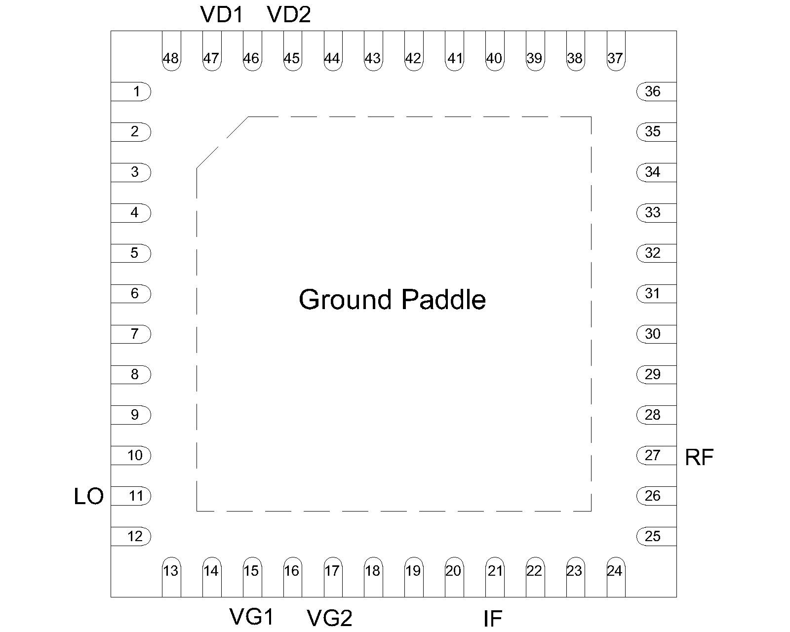
Port Diagram
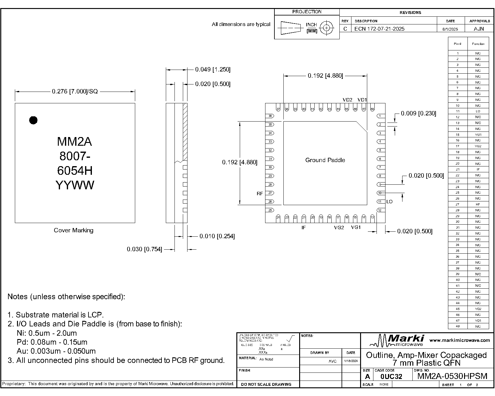
A top-down x-ray view of the MM2A-0530HPSM’s PSM package outline drawing is shown below. The MM2A-0530HPSM has the input and output ports given in Port Functions.
Sales: 408-778-9952 | General: 408-778-4200 | Fax: 408-778-4300
Sales & Customer Support: [email protected]
Tech Support: [email protected]
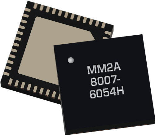
The MM2A-0530HPSM is a versatile, robust, and broadband triple balanced mixer with an integrated broadband LO driver amplifier. The MM2A-0530HPSM is ideal for applications with wide and overlapping bandwidths and operation through the K band. The integrated LO driver amplifier allows for operation with LO powers as low as +0dBm while retaining exceptional conversion loss and linearity.

| Part Number | Description | Package | Green Status | Product Lifecycle | Export Classification |
|---|---|---|---|---|---|
| MM2A-0530HPSM | Integrated Drive GaAs MMIC Mixer | QFN | REACH RoHS | Released | EAR99 |
| EVB-MM2A-0530HP | Evaluation Board, Integrated Drive GaAs MMIC Mixer | EVB | RoHS REACH | Released | EAR99 |
MM2A-0530HPSM
Integrated Drive GaAs MMIC Mixer
| Revision Code | Revision Date | Comment |
|---|---|---|
| - | 2024-05-06 | Initial Release |
| A | 2024-11-21 | Updated 2D outline drawing per ECN#24129. Corrected number of decimal places in dimensions. |
| B | 2025-08-04 | Updated outline drawing per ECN #172-07-21-2025. Corrected RF and IF pin location. |
MM2A-0530HPSM
Integrated Drive GaAs MMIC Mixer
A top-down x-ray view of the MM2A-0530HPSM’s PSM package outline drawing is shown below. The MM2A-0530HPSM has the input and output ports given in Port Functions.
MM2A-0530HPSM
Integrated Drive GaAs MMIC Mixer
| Port | Function | Description | DC Equivalent Circuit |
|---|---|---|---|
| Pin 11 | LO Input | Pin 11 is DC open and AC matched to 50Ω over the specified LO frequency range. |  |
| Pin 15 | Vg1 | Pin 15 provides bias for an internal current mirror that sets the current draw for amplifier input stage. Increasing current will increase gain at the expense of efficiency. The default series resistor (270 Ohms) is chosen to optimize gain, output power and efficiency when Vg1 and Vd1 are both tied to 5V. |  |
| Pin 17 | Vg2 | Pin 17 provides bias for an internal current mirror that sets the current draw for amplifier output stage. Increasing current will increase gain at the expense of efficiency. The default series resistor (82.5 Ohms) is chosen to optimize gain, output power and efficiency when Vg2 and Vd2 are both tied to 5V. |  |
| Pin 21 | IF | Pin 21 is diode coupled and AC matched to 50Ω over the specified IF port frequency range. |  |
| Pin 27 | RF Input / Output | Pin 27 is DC short and AC matched to 50Ω over the specified RF frequency range. |  |
| Pin 45 | Vd2 | Pin 45 is the DC supply pin for the amplifier’s output stage. |  |
| Pin 47 | Vd1 | Pin 47 is the DC supply pin for the amplifier’s input stage. | |
MM2A-0530HPSM
Integrated Drive GaAs MMIC Mixer
The Absolute Maximum Ratings indicate limits beyond which damage may occur to the device. If any one of these limits are exceeded, the device may become inoperable or have a reduced lifetime. Reliability limits are individual, instantaneous catastrophic limits only. Functional operation limits are indicated below. Operation of the device at multiple absolute maximum limits or for extended periods at a single limit can cause degradation and damage to the device.
| Parameter | Maximum Rating | Unit |
|---|---|---|
| Bias Current (Ig1+Ig2) | 95 | mA |
| Bias Voltage (Vg1,Vg2) | 6 | V |
| DC Current (IF) | 30 | mA |
| Drain Current (Id1+Id2) | 400 | mA |
| Drain Supply Voltage (Vd1,Vd2) | 6 | V |
| Maximum Operating Temperature | 85 | °C |
| Maximum Storage Temperature | 125 | °C |
| Minimum Operating Temperature | -40 | °C |
| Minimum Storage Temperature | -65 | °C |
| Power Handling, at any Port | 15 | dBm |
| Parameter | Details | Rating |
|---|---|---|
| Dimensions | - | 7x7 mm |
| Moisture Sensitivity Level | - | MSL 1 |
The Recommended Operating Conditions indicate the limits, inside which the device should be operated, to guarantee the performance given in Electrical Specifications Operating outside these limits may not necessarily cause damage to the device, but the performance may degrade outside the limits of the electrical specifications. For limits, above which damage may occur, see Absolute Maximum Ratings.
| Parameter | Min | Nominal | Max | Unit |
|---|---|---|---|---|
| Positive DC Voltage | - | 5 | - | V |
| LO Input Power | -3 | 0 | 3 | - |
| Power Supply DC Current (Ig) (No RF Input) | 11 | 19 | 23 | mA |
| Power Supply DC Current (Id) (No RF Input) | 121 | 218 | 259 | mA |
MM2A-0530HPSM
Integrated Drive GaAs MMIC Mixer
The electrical specifications apply at TA=+25°C in a 50Ω system. Typical data shown is for a down conversion application with a +0dBm LO input to the integrated LO driver amp biased at +5Vd1/+5Vd2/+5Vg1/+5Vg2 unless otherwise specified.
| Parameter | Test Conditions | Min | Typ | Max | Unit |
|---|---|---|---|---|---|
| Conversion Loss | RF/LO = 5 - 30 GHz
I = 2 - 22 GHz | - | 8 | - | dB |
| IF Frequency Range | - | 2 | - | 22 | GHz |
| Input IP3 | RF/LO = 5 - 30 GHz
I = 2 - 22 GHz | - | 25 | - | dBm |
| Input P1dB | - | - | 15 | - | dBm |
| LO Frequency Range | - | 5 | - | 30 | GHz |
| LO Leakage, LO to IF | RF/LO = 5 - 30 GHz | - | 24 | - | dBm |
| LO Leakage, LO to RF | RF/LO = 5 - 30 GHz | - | 23 | - | dBm |
| Noise Figure | RF/LO = 5 - 30 GHz
I = 2 - 22 GHz | - | 8 | - | dB |
| RF Frequency Range | - | 5 | - | 30 | GHz |
| RF-IF Isolation | RF/LO = 5 - 30 GHz | - | 39 | - | dB |
Eval board IF and RF traces were de-embedded using AFR and LO trace power correction was applied to show the true performance of the QFN. Measured as a down converter, unless otherwise stated Mixer Noise Figure typically measures within 0.5 dB of conversion loss for IF frequencies greater than 5 MHz.
MM2A-0530HPSM
Integrated Drive GaAs MMIC Mixer


MM2A-0530HPSM
Integrated Drive GaAs MMIC Mixer


MM2A-0530HPSM
Integrated Drive GaAs MMIC Mixer


MM2A-0530HPSM
Integrated Drive GaAs MMIC Mixer

MM2A-0530HPSM
Integrated Drive GaAs MMIC Mixer
MM2A-0530HPSM
Integrated Drive GaAs MMIC Mixer
Download : Footprint Drawing

MM2A-0530HPSM
Integrated Drive GaAs MMIC Mixer