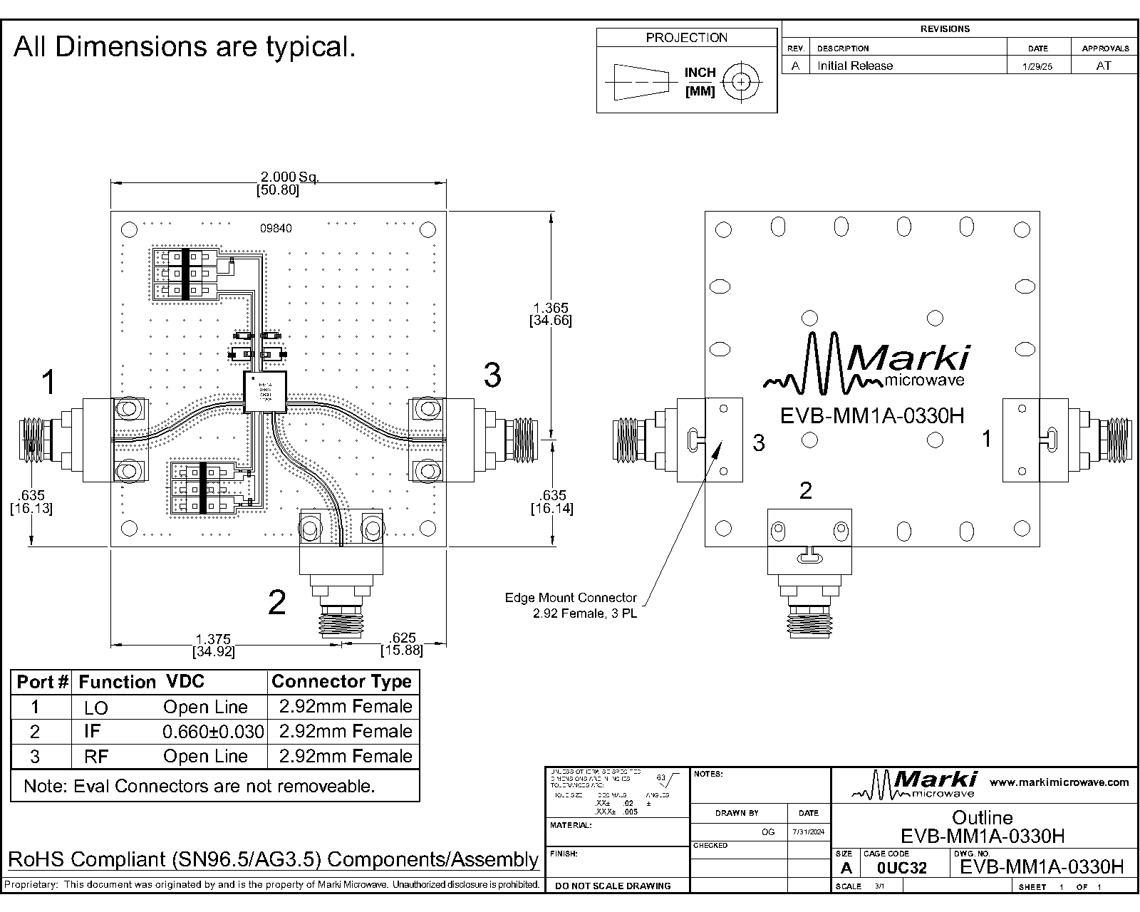
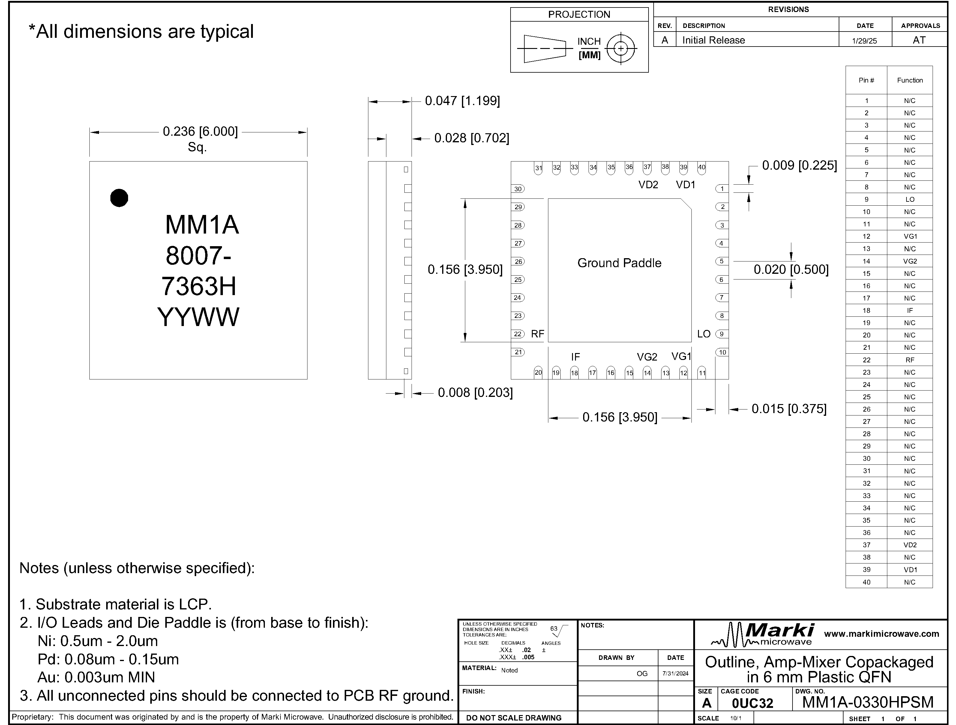
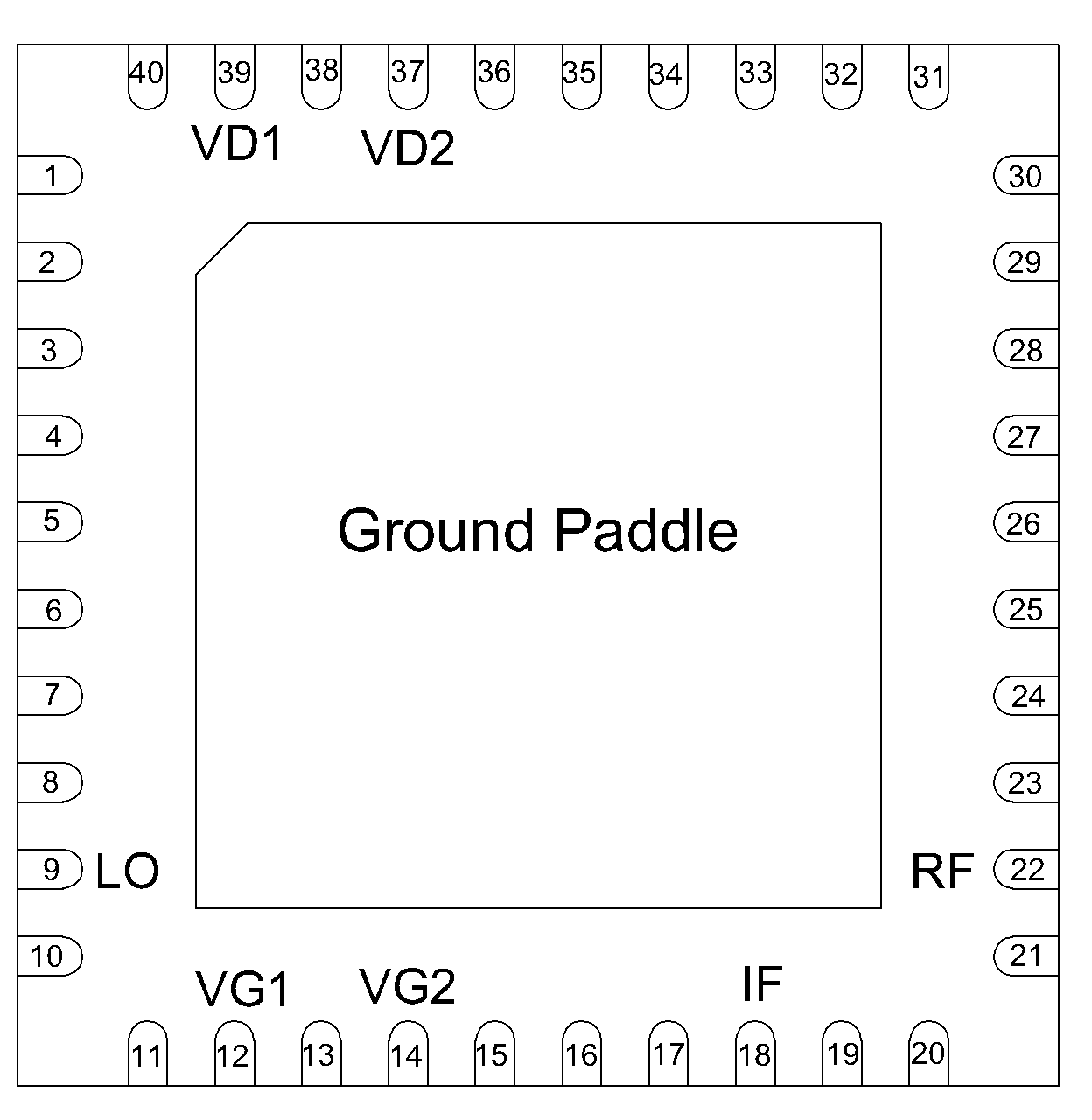
Port Diagram
A top-down x-ray view of the MM1A-0330HPSM’s PSM package outline drawing is shown below. The MM1A-0330HPSM has the input and output ports given in Port Functions.
Sales: 408-778-9952 | General: 408-778-4200 | Fax: 408-778-4300
Sales & Customer Support: [email protected]
Tech Support: [email protected]
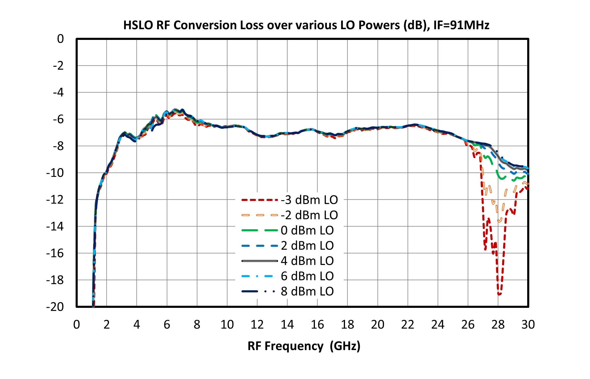
The MM1A-0330HPSM is a versatile, robust, and broadband double balanced mixer with an integrated broadband LO driver amplifier. The MM1A-0330HSM is ideal for applications with wide bandwidths and operation through the K band. The integrated LO driver amplifier allows for operation with LO powers as low as -2 dBm while retaining exceptional conversion loss and linearity.
RF/LO response: 3GHz - 30GHz
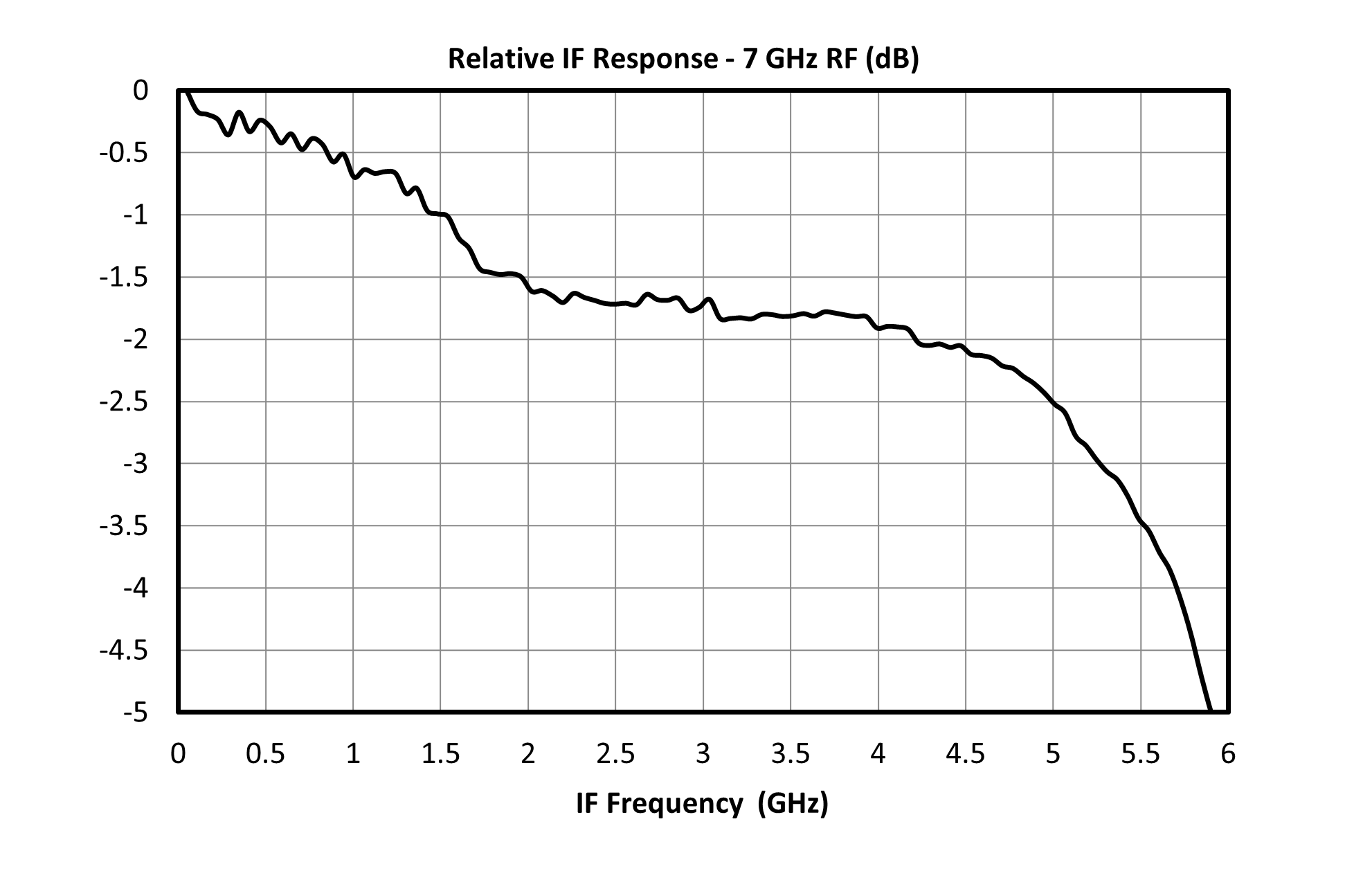
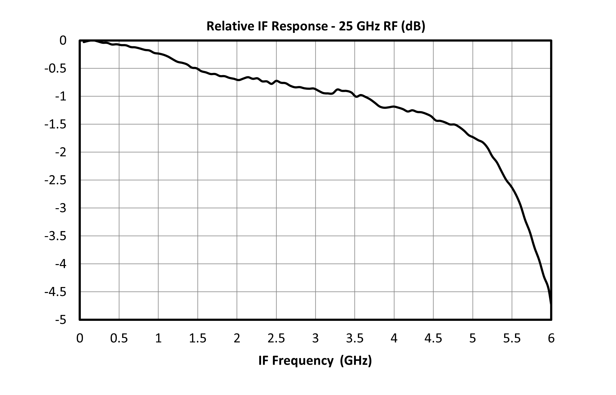
IF response: DC – 5GHz
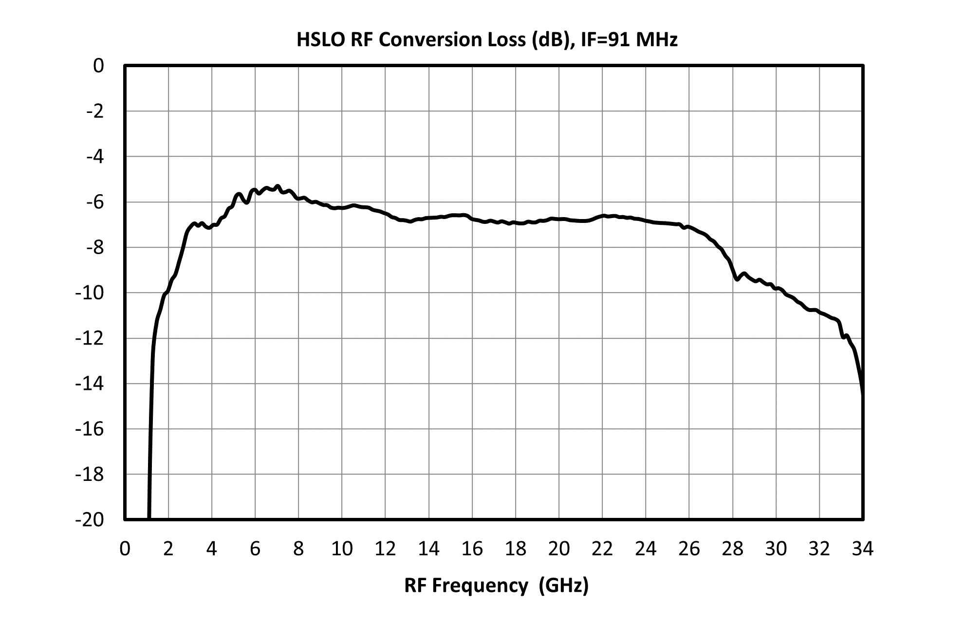
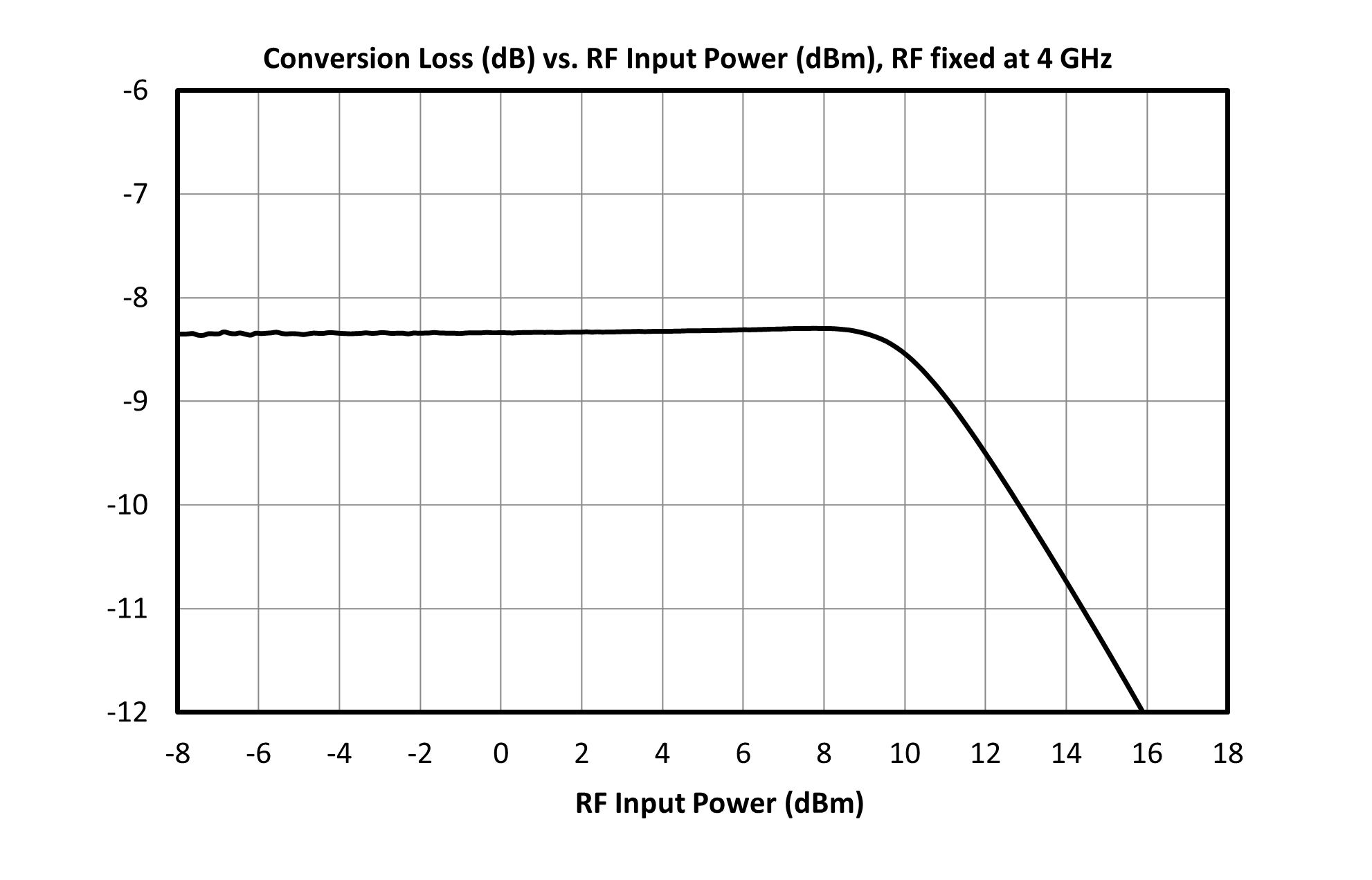
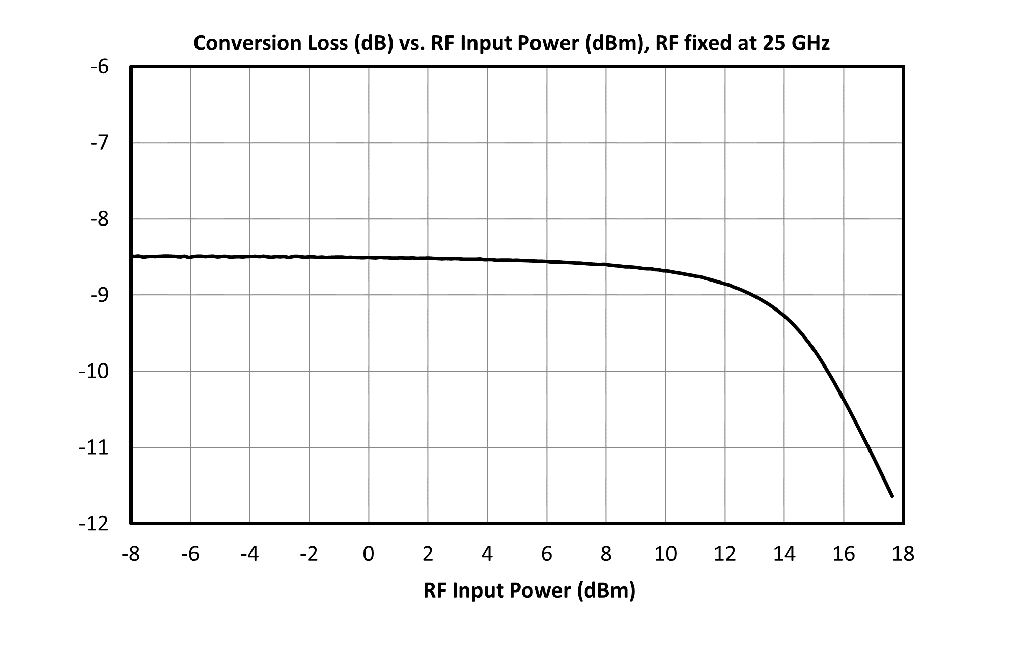
Conversion Loss: 7dB
Minimum LO drive: -2dBm

| Part Number | Description | Package | Green Status | Product Lifecycle | Export Classification |
|---|---|---|---|---|---|
| MM1A-0330HPSM | Double Balanced Mixer/LO Amplifier | QFN | REACH RoHS | Released | EAR99 |
| EVB-MM1A-0330H | Evaluation Board, Integrated Drive GaAs MMIC Mixer | EVB | REACH RoHS | Released | EAR99 |
MM1A-0330HPSM
Double Balanced Mixer/LO Amplifier
| Revision Code | Revision Date | Comment |
|---|---|---|
| - | 2024-12-10 | Initial Release |
MM1A-0330HPSM
Double Balanced Mixer/LO Amplifier
A top-down x-ray view of the MM1A-0330HPSM’s PSM package outline drawing is shown below. The MM1A-0330HPSM has the input and output ports given in Port Functions.
MM1A-0330HPSM
Double Balanced Mixer/LO Amplifier
| Port | Function | Description | DC Equivalent Circuit |
|---|---|---|---|
| Pin 12 | Vg1 | Pin 12 provides bias for an internal current mirror that sets the current draw for amplifier input stage. Increasing current will increase gain at the expense of efficiency. The default series resistor (270 Ohms) is chosen to optimize gain, output power and efficiency when Vg1 and Vd1 are both tied to 5V. | - |
| Pin 14 | Vg2 | Pin 14 provides bias for an internal current mirror that sets the current draw for amplifier output stage. Increasing current will increase gain at the expense of efficiency. The default series resistor (82.5 Ohms) is chosen to optimize gain, output power and efficiency when Vg2 and Vd2 are both tied to 5V. | - |
| Pin 18 | IF | Pin 18 is diode coupled and AC matched to 50Ω over the specified IF port frequency range. | - |
| Pin 22 | RF Input / Output | Pin 22 is DC short and AC matched to 50Ω over the specified RF frequency range. | - |
| Pin 37 | Vd2 | Pin 37 is the DC supply pin for the amplifier’s output stage. | - |
| Pin 39 | Vd1 | Pin 39 is the DC supply pin for the amplifier’s input stage. | - |
| Pin 9 | LO Input | Pin 9 is DC open and AC matched to 50Ω over the specified LO frequency range. | - |
MM1A-0330HPSM
Double Balanced Mixer/LO Amplifier
The Absolute Maximum Ratings indicate limits beyond which damage may occur to the device. If these limits are exceeded, the device may be inoperable or have a reduced lifetime. All Absolute Maximum Ratings are individual and should not be met in parallel.
| Parameter | Maximum Rating | Unit |
|---|---|---|
| Bias Current (Ig1+Ig2) | 95 | mA |
| Bias Voltage (Vg1,Vg2) | 6 | V |
| Drain Current (Id1+Id2) | 400 | mA |
| Drain Supply Voltage (Vd1,Vd2) | 6 | V |
| Maximum Operating Temperature | 85 | °C |
| Maximum Storage Temperature | 125 | °C |
| Minimum Operating Temperature | -40 | °C |
| Minimum Storage Temperature | -65 | °C |
| Pin 18 DC Current (RF) | 15 | mA |
| Power Handling, at any Port | 15 | dBm |
| Parameter | Details | Rating |
|---|---|---|
| Dimensions | - | 6 x 6 mm |
| Moisture Sensitivity Level | - | MSL 1 |
The Recommended Operating Conditions indicate the limits, inside which the device should be operated, to guarantee the performance given in Electrical Specifications Operating outside these limits may not necessarily cause damage to the device, but the performance may degrade outside the limits of the electrical specifications. For limits, above which damage may occur, see Absolute Maximum Ratings.
| Parameter | Min | Nominal | Max | Unit |
|---|---|---|---|---|
| Ambient Temperature | -40 | 25 | 85 | °C |
| LO Input Power | -2 | 0 | 8 | dBm |
| Power Supply DC Current (Id1+Id2) (No RF Input) | 121 | 218 | 259 | mA |
| Positive DC Voltage (Vd1, Vd2) | - | 5 | - | V |
| Power Supply DC Current (Ig1+Ig2) (No RF Input) | 11 | 19 | 23 | mA |
| Power Supply DC Voltage (Vg1,Vg2) | - | 5 | - | V |
MM1A-0330HPSM
Double Balanced Mixer/LO Amplifier
The electrical specifications apply at TA=+25°C in a 50Ω system. Typical data shown is for a down conversion application with a +4dBm LO input to the integrated LO driver amp biased at Vd1=Vd2=Vg1=Vg2=+5V unless otherwise specified.
| Parameter | Test Conditions | Min | Typ | Max | Unit |
|---|---|---|---|---|---|
| Conversion Loss 1 | RF/LO = 3 - 30 GHz I = 91MHz | - | 7 | - | dB |
| Conversion Loss 2 | RF/LO = 3 - 30 GHz I = DC – 5 GHz | - | 8 | - | dB |
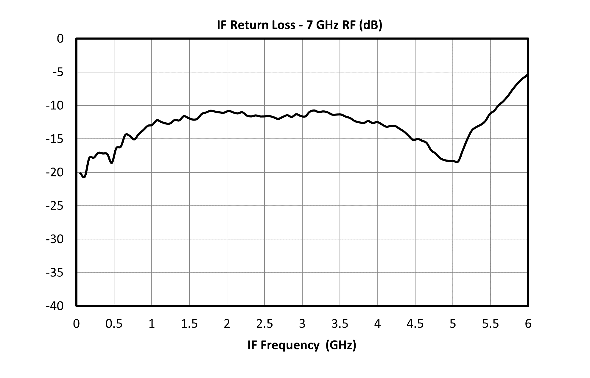
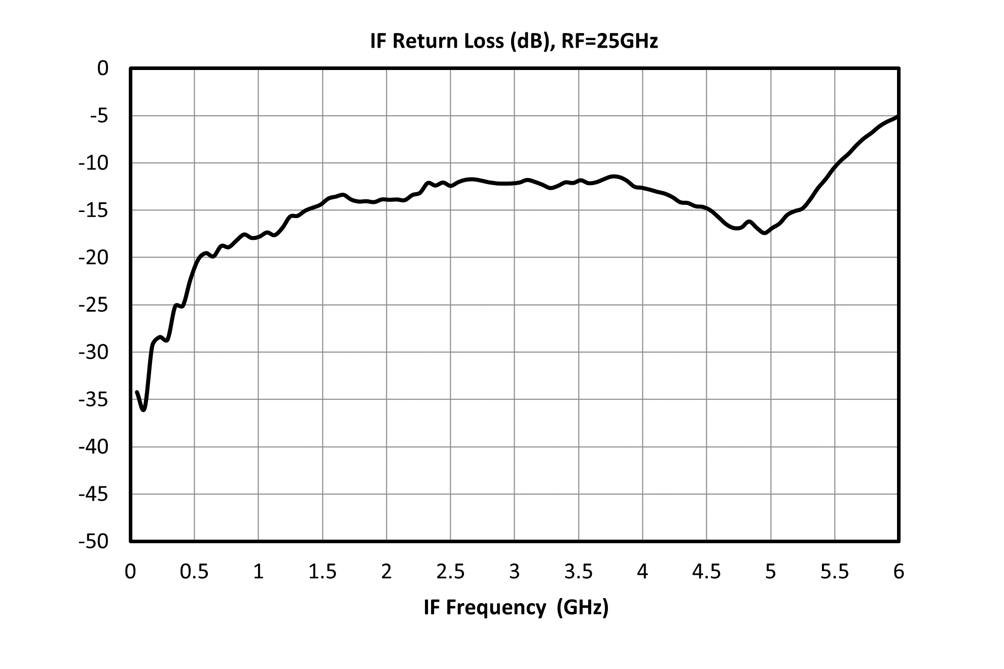
| IF Frequency Range | - | 0 | - | 5 | GHz |
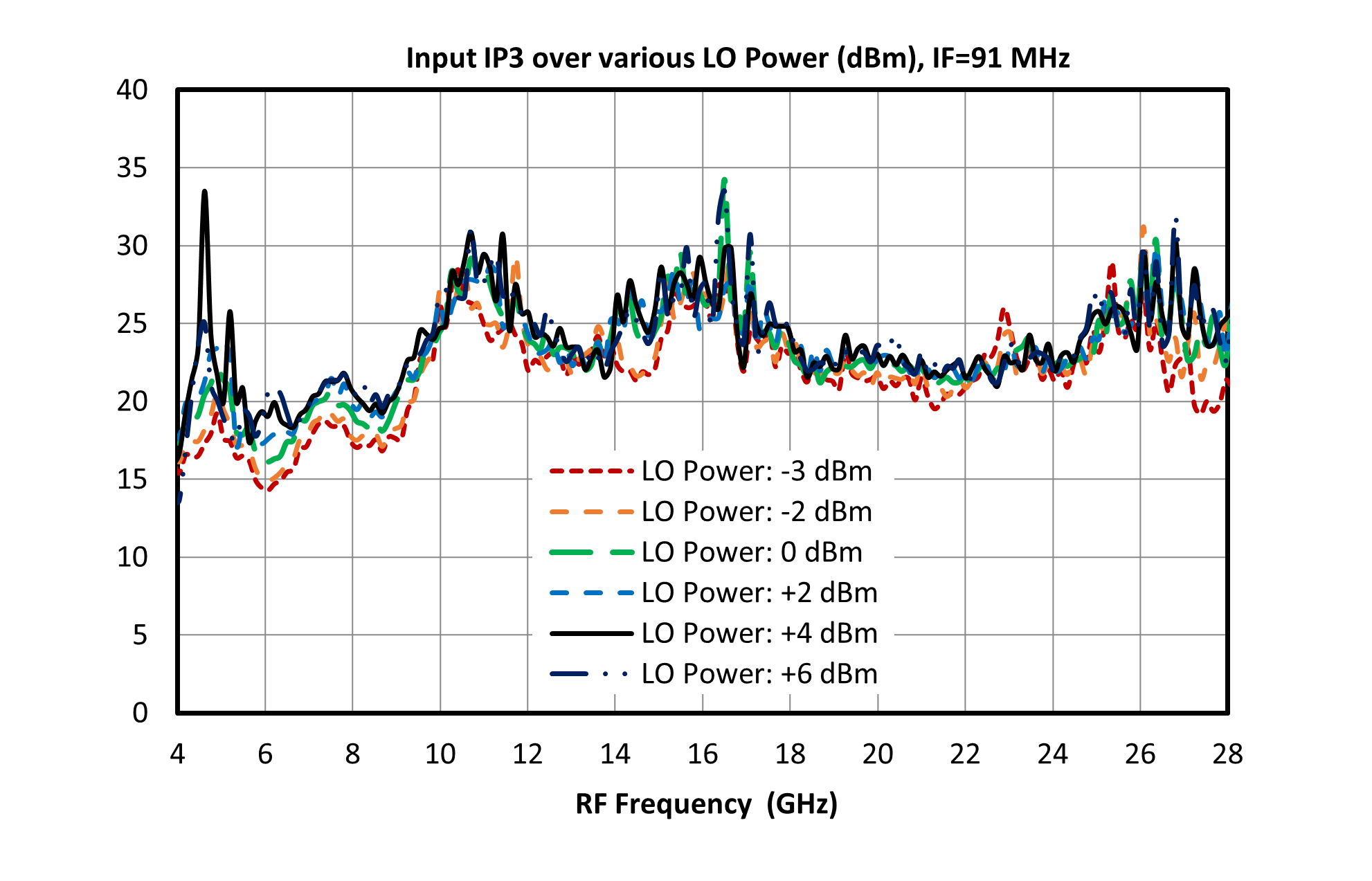
| Input IP3 | RF/LO = 3 - 30 GHz I = 91 MHz | - | 23 | - | dBm |
| Input P1dB | RF = 25GHz, IF = 91MHz, HSLO=25.091GHz | - | 13.5 | - | dBm |
| Input P1dB | RF = 4GHz, IF = 91MHz, HSLO=4.091GHz | - | 13.5 | - | dBm |
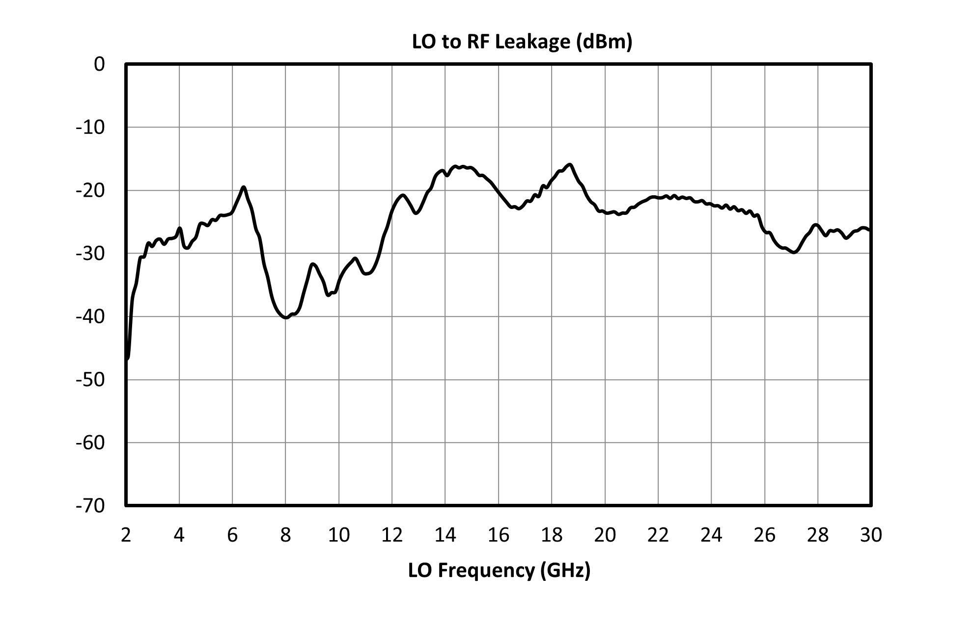
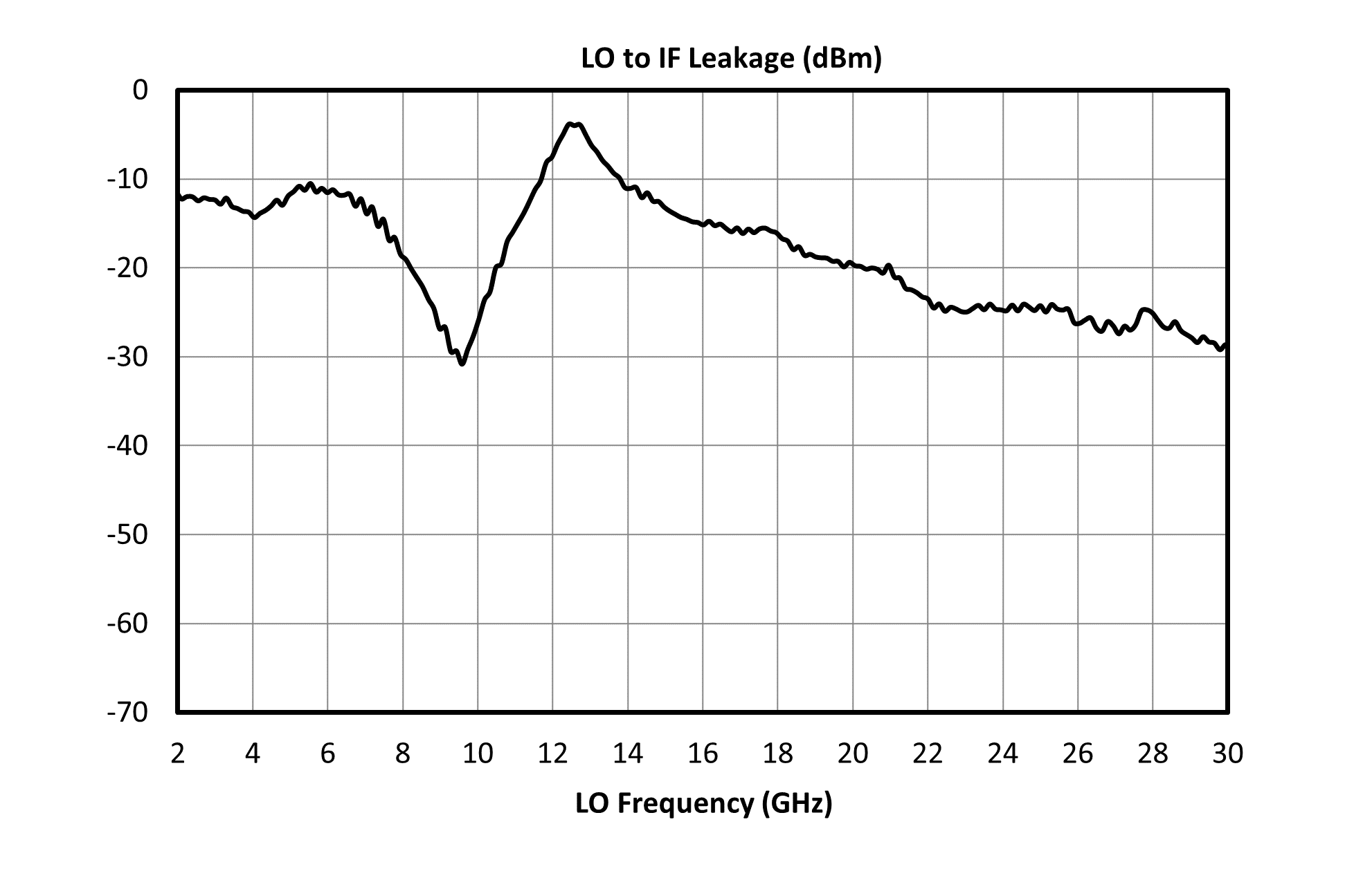
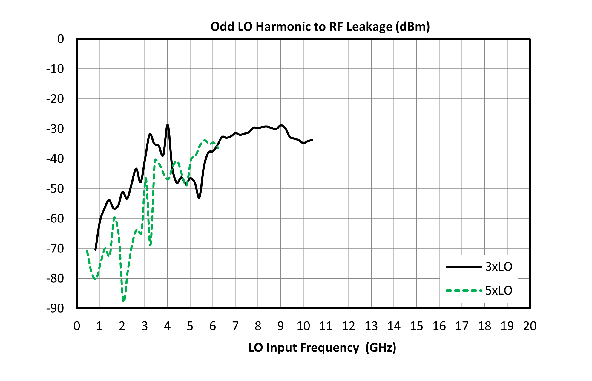
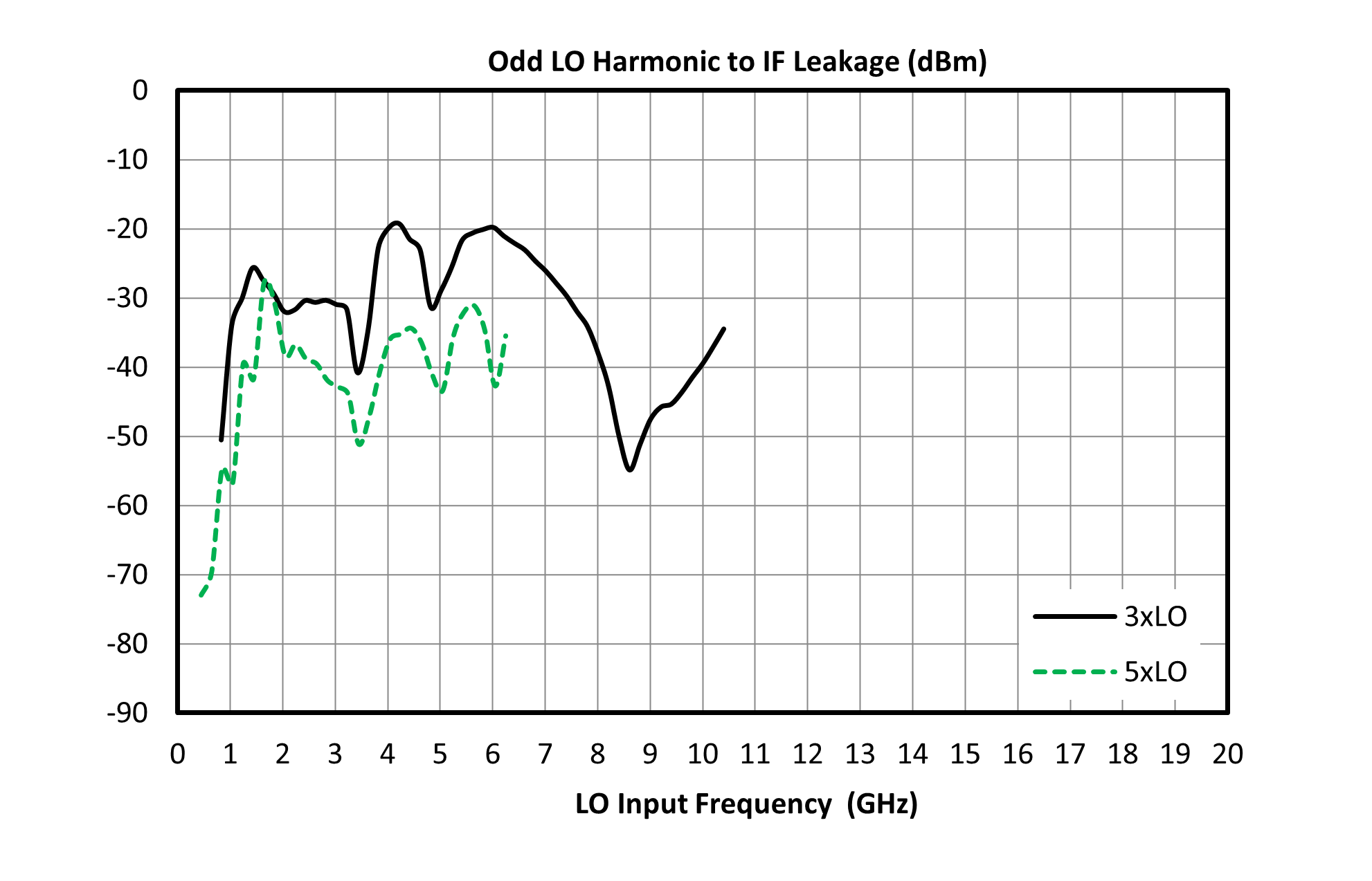
| LO Frequency Range | - | 3 | - | 30 | GHz |
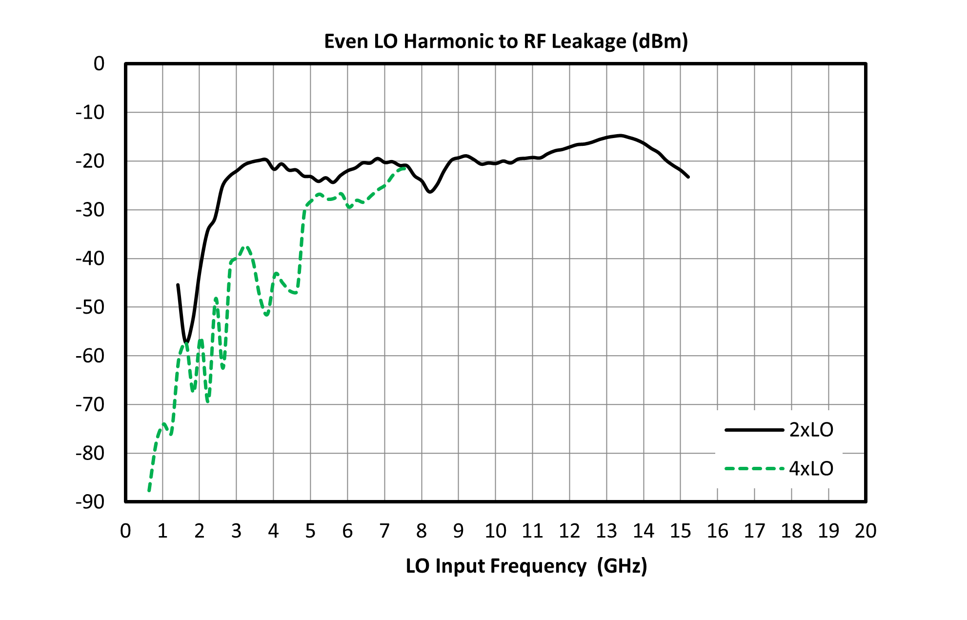
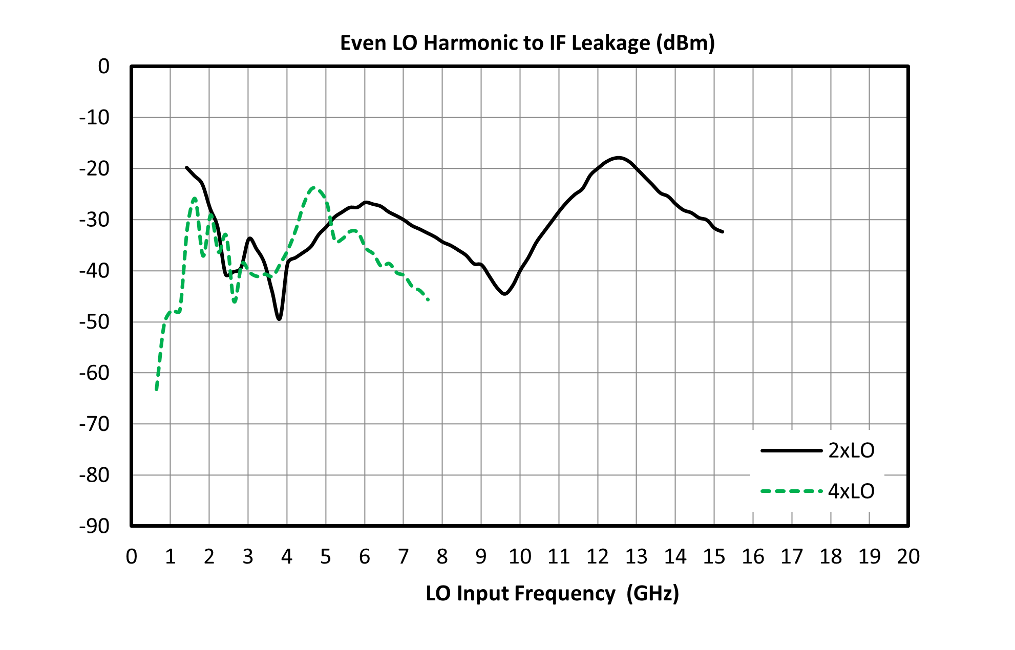
| LO Leakage, LO to IF | LO= 3 - 30 GHz | - | 18 | - | dBm |
| LO Leakage, LO to RF | LO= 3 - 30 GHz | - | 24 | - | dBm |
| Noise Figure 3 | RF/LO = 3 - 30GHz I = DC – 5 GHz | - | 7 | - | dB |
| RF Frequency Range | - | 3 | - | 30 | GHz |
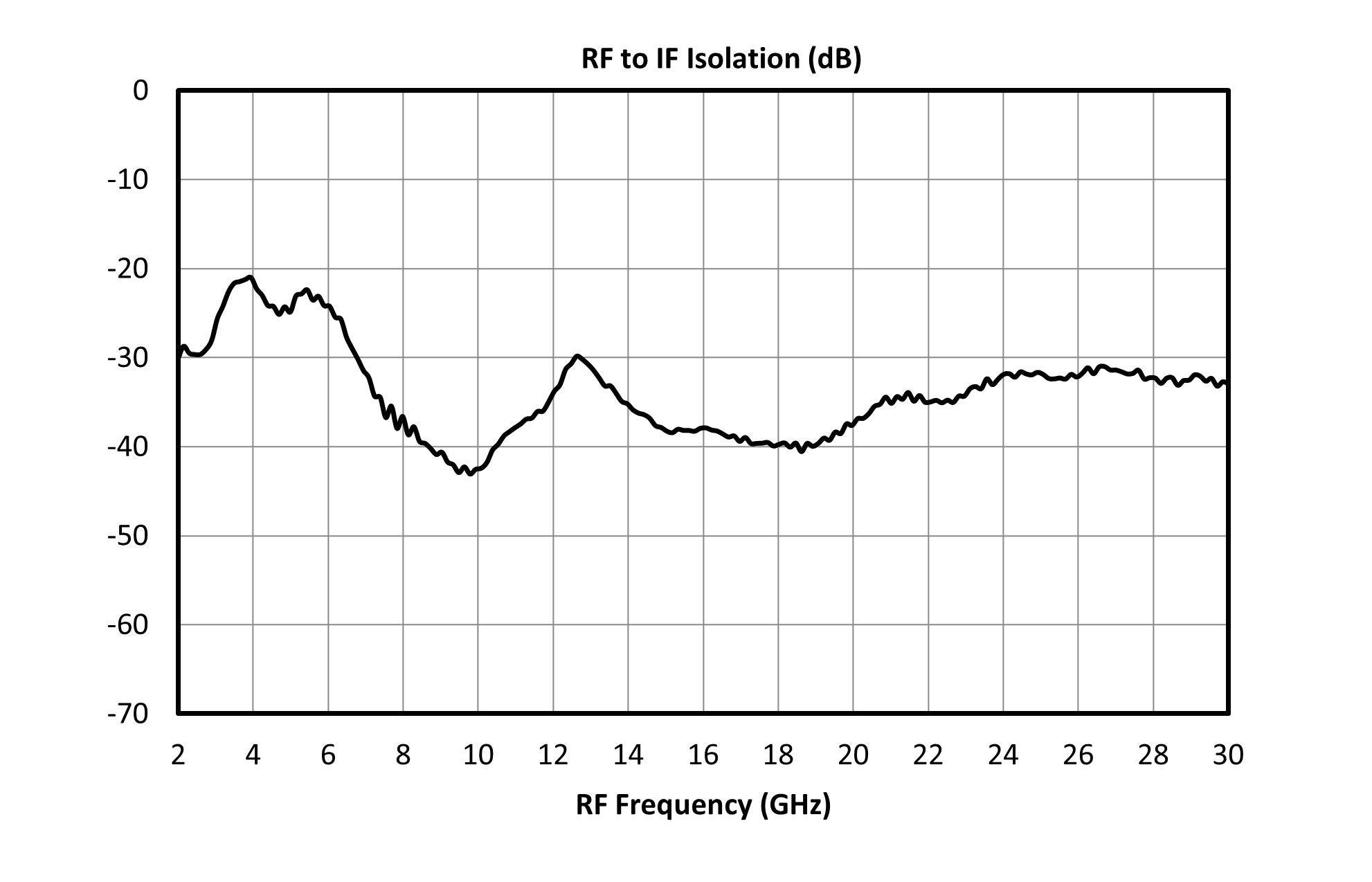
| RF-IF Isolation | RF = 3 - 30 GHz | - | 34 | - | dB |
| Parameter | Test Conditions | Min | Typ | Max | Unit |
|---|---|---|---|---|---|
| Conversion Loss 1 | RF/LO = 3 - 30 GHz I = 91MHz | - | 7 | - | dB |
| Conversion Loss 2 | RF/LO = 3 - 30 GHz I = DC – 5 GHz | - | 8 | - | dB |
| IF Frequency Range | - | 0 | - | 5 | GHz |
| Input IP3 | RF/LO = 3 - 30 GHz I = 91 MHz | - | 23 | - | dBm |
| Input P1dB | RF = 25GHz, IF = 91MHz, HSLO=25.091GHz | - | 13.5 | - | dBm |
| Input P1dB | RF = 4GHz, IF = 91MHz, HSLO=4.091GHz | - | 13.5 | - | dBm |
| LO Frequency Range | - | 3 | - | 30 | GHz |
| LO Leakage, LO to IF | LO= 3 - 30 GHz | - | 18 | - | dBm |
| LO Leakage, LO to RF | LO= 3 - 30 GHz | - | 24 | - | dBm |
| Noise Figure 3 | RF/LO = 3 - 30GHz I = DC – 5 GHz | - | 7 | - | dB |
| RF Frequency Range | - | 3 | - | 30 | GHz |
| RF-IF Isolation | RF = 3 - 30 GHz | - | 34 | - | dB |
[1] Measured as a down converter to a fixed IF = 91 MHz. EVB IF and RF trace losses de-embedded.
[2] Measured as a down converter. EVB IF and RF trace losses de-embedded.
[3] Mixer Noise Figure typically measures within 0.5 dB of conversion loss for IF frequencies greater than 5 MHz.
MM1A-0330HPSM
Double Balanced Mixer/LO Amplifier
MM1A-0330HPSM
Double Balanced Mixer/LO Amplifier


MM1A-0330HPSM
Double Balanced Mixer/LO Amplifier
MM1A-0330HPSM
Double Balanced Mixer/LO Amplifier

MM1A-0330HPSM
Double Balanced Mixer/LO Amplifier
MM1A-0330HPSM
Double Balanced Mixer/LO Amplifier
Download : Footprint Drawing

MM1A-0330HPSM
Double Balanced Mixer/LO Amplifier