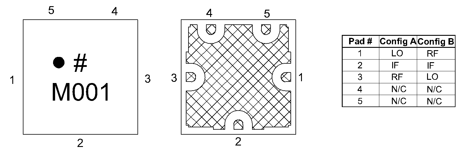
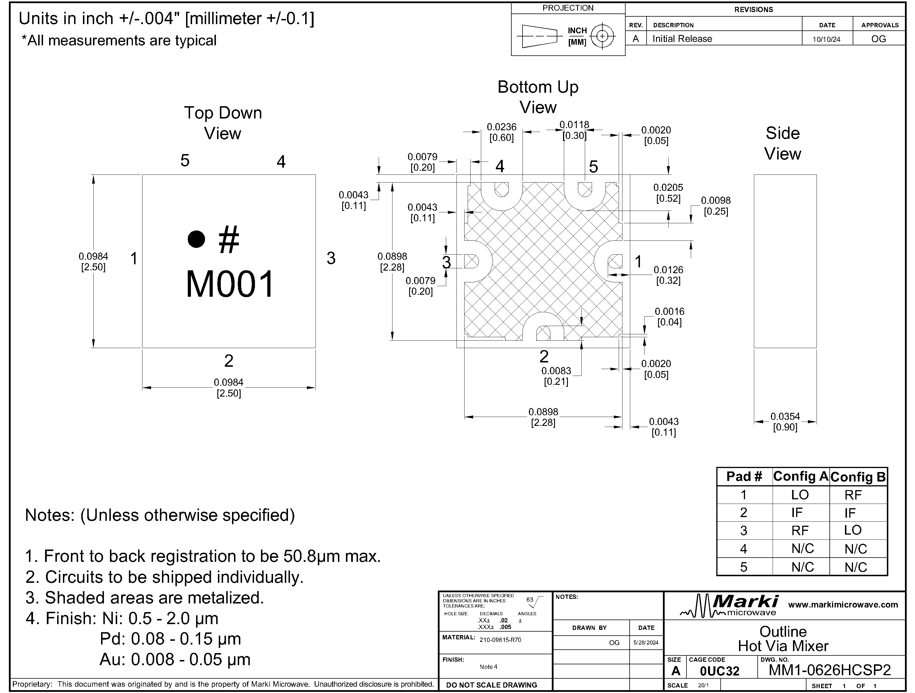
Device Overview

General Description

The MM1-0626HCSP2 is a highly linear passive GaAs double balanced MMIC mixer suitable for both up and down-conversion applications. As with all Marki Microwave mixers, it features excellent conversion loss, isolation and spurious performance across a broad bandwidth and in a small form factor. The MM1-0626HCSP2 is available in a lead-free, RoHS compliant 2.5x2.5 mm chip scale surface mount package (CSP2) and is compatible with standard leaded and lead-free PCB reflow soldering processes. The MM1-0626HCSP2 is a smaller alternative to the standard MM1-0626HSM.

Photo of MM1-0626HCSP2

Features

  • Compact 2.5x2.5 mm Chip Scale Package
  • Broadband Performance
  • Excellent Unit-to-Unit Repeatability
  • RoHS Compliant

Applications

  • Test and Measurement Equipment
  • SATCOM
  • Electronic Warfare
  • 5G

Functional Block Diagram

Block Diagram

Part Ordering Options

Part NumberDescriptionPackageGreen StatusProduct LifecycleExport Classification
MM1-0626HCSP2GaAs MMIC Chip Scale Package Double Balanced MixerCSP2

REACH

RoHS

ReleasedEAR99
EVB-MM1-0626HCSP Double Balanced Mixer Evaluation BoardEVB

REACH

RoHS

ReleasedEAR99

Table Of Contents

Revision History

Revision CodeRevision DateComment
-2024-07-30Initial Release
A2025-04-28Updated Moisture Sensitivity from MSL3 to MSL1

Rev: A | Copyright © 2024 - 2025 Marki Microwave LLC.

2

Port Configuration and Functions

Port Diagram

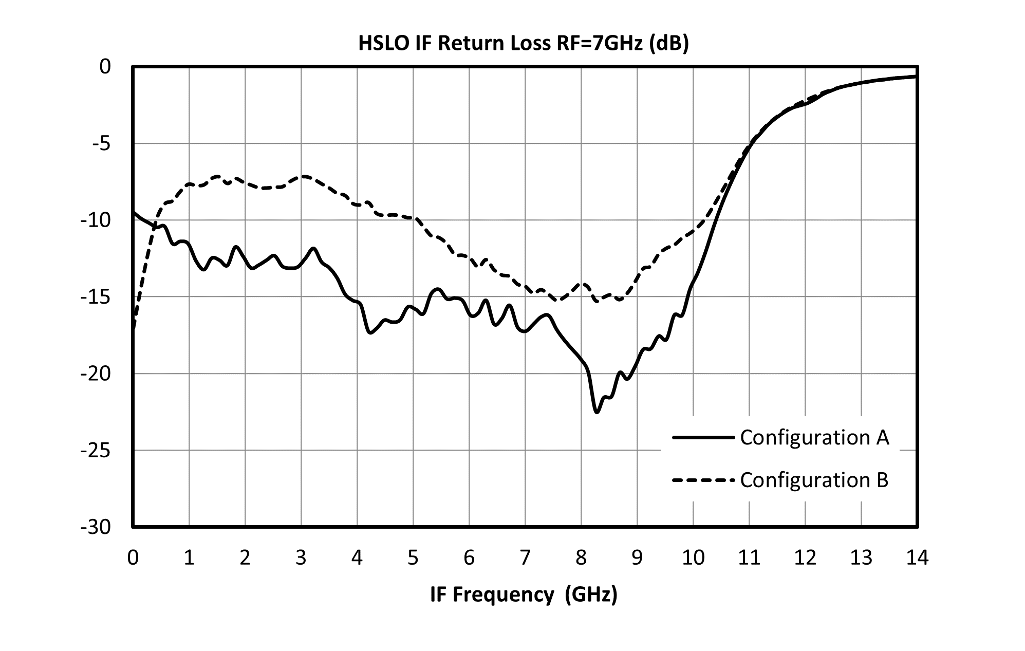
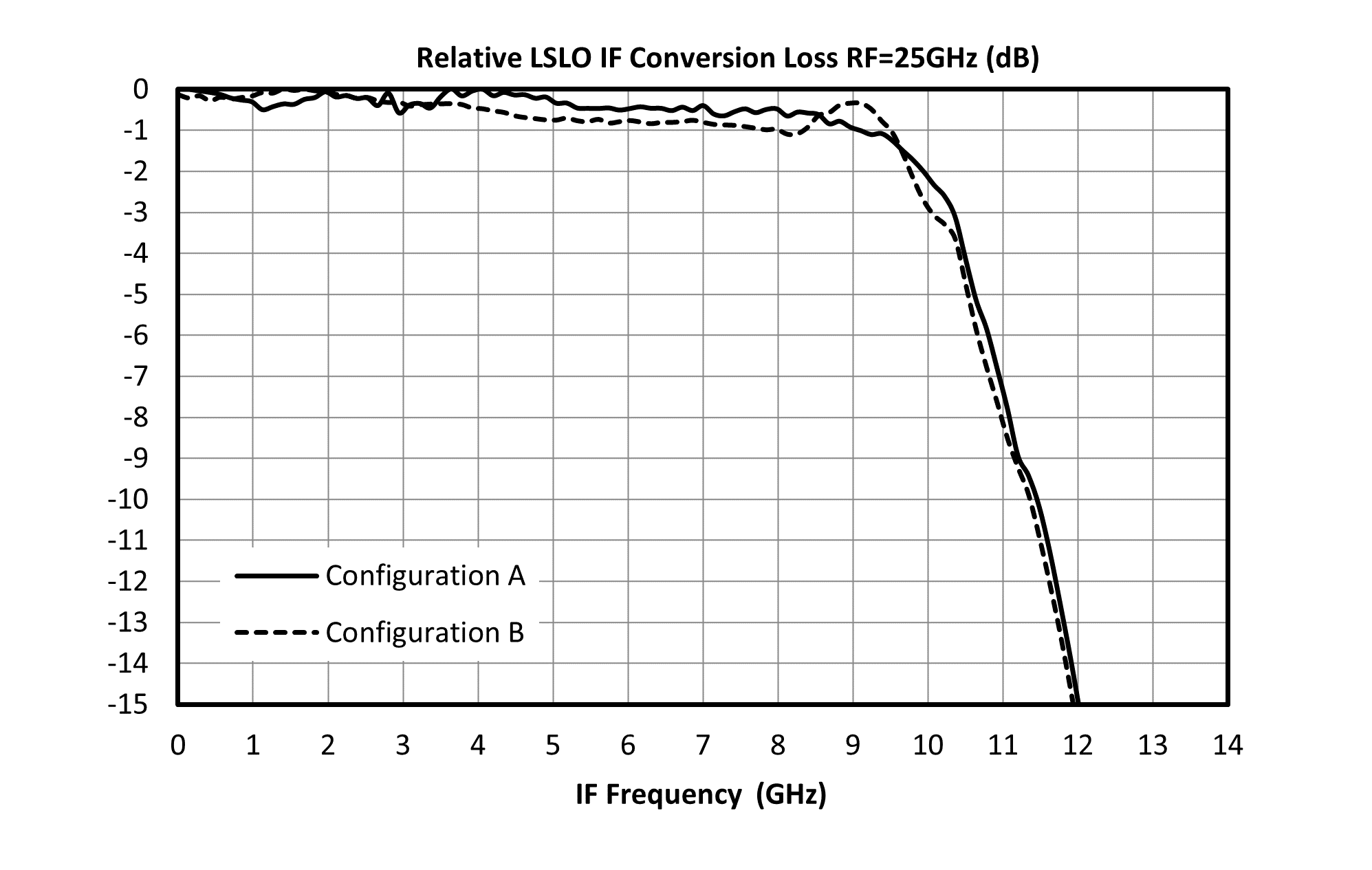
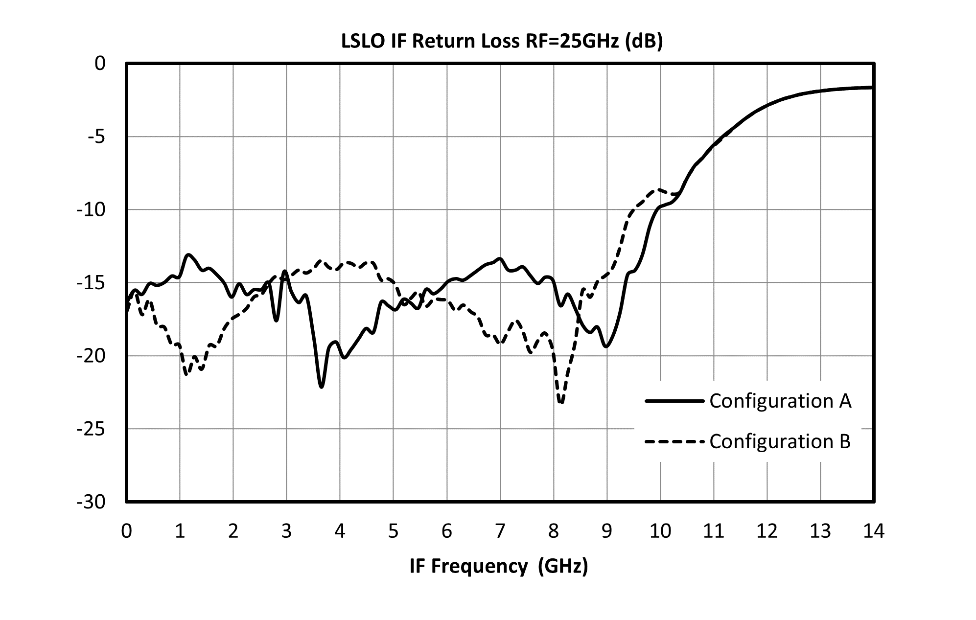
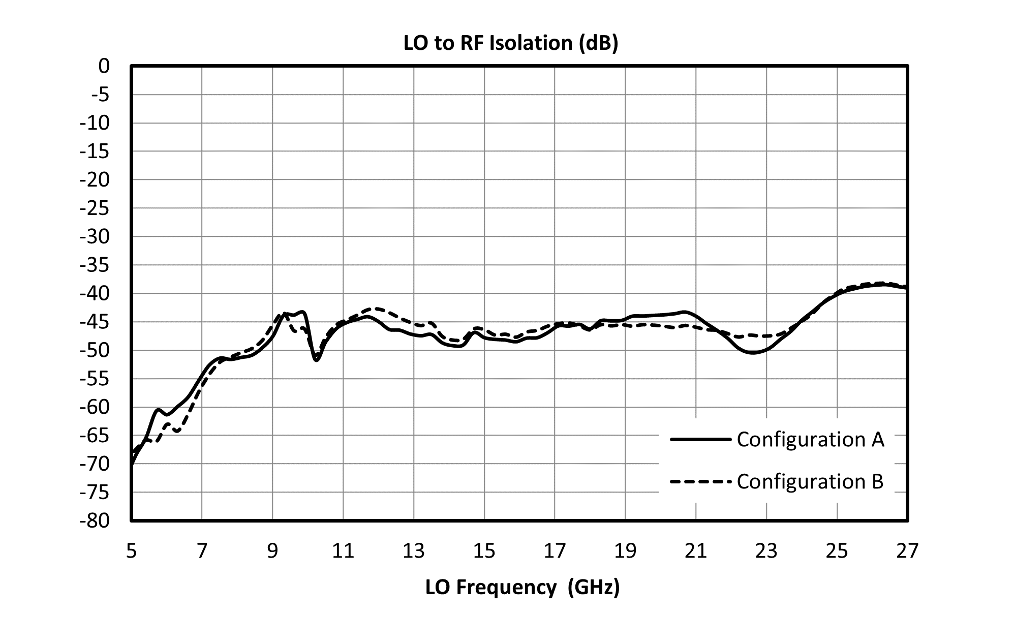
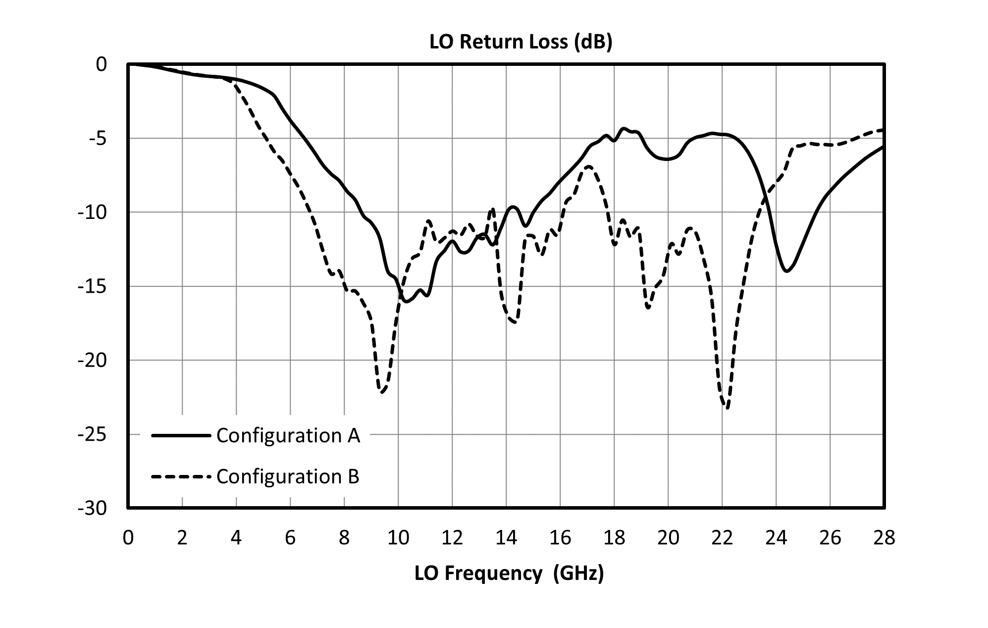
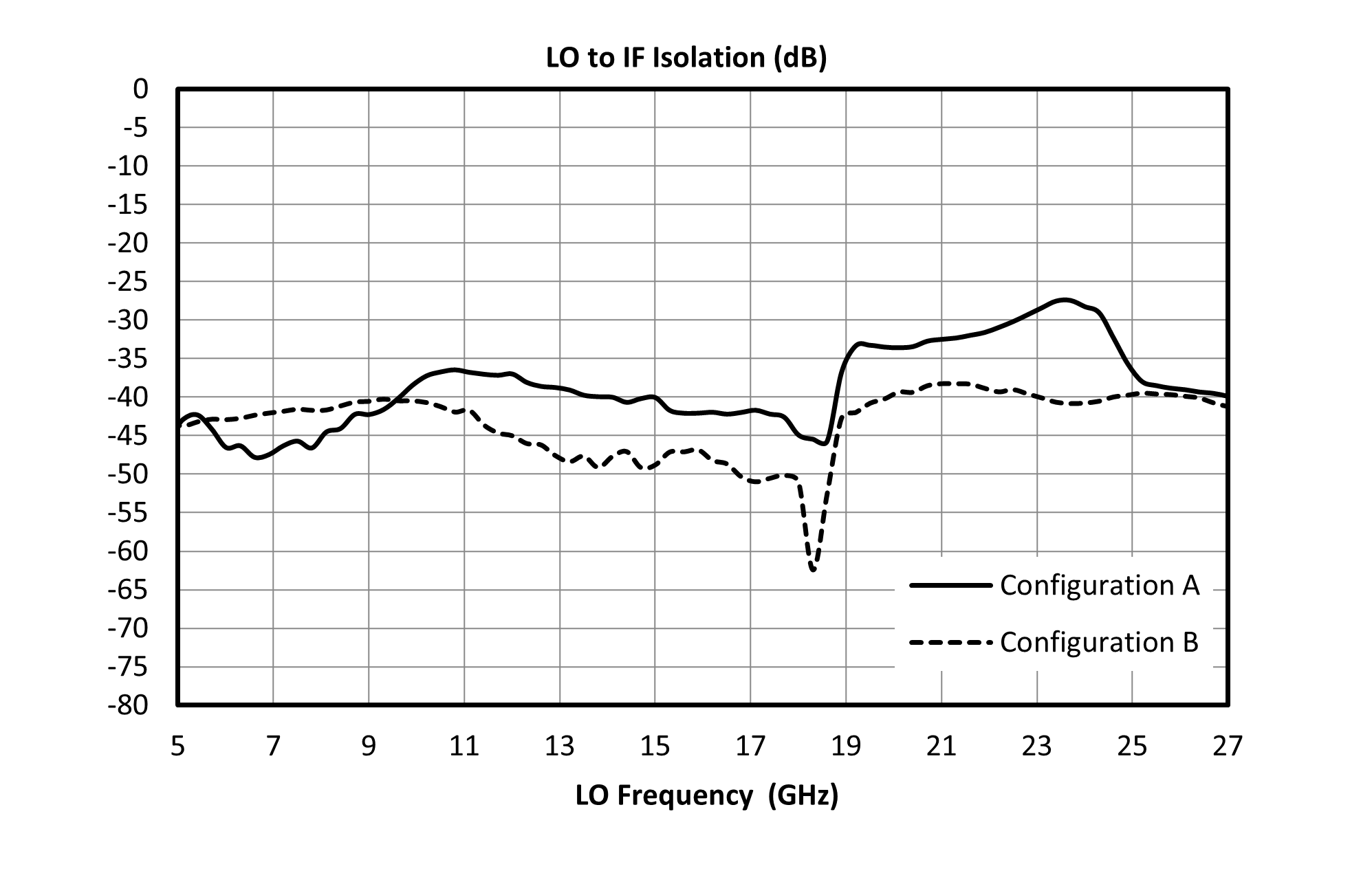
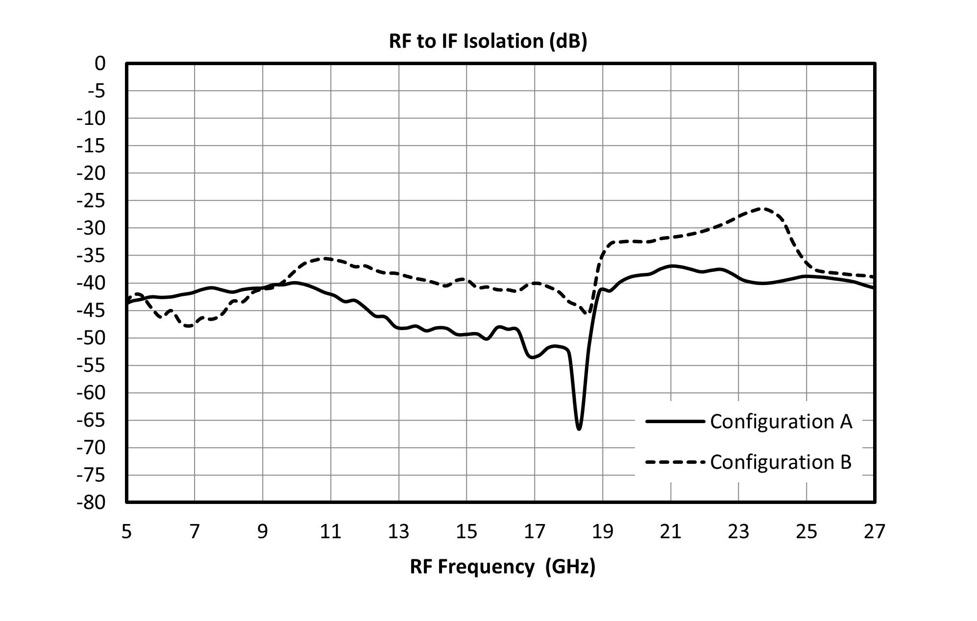
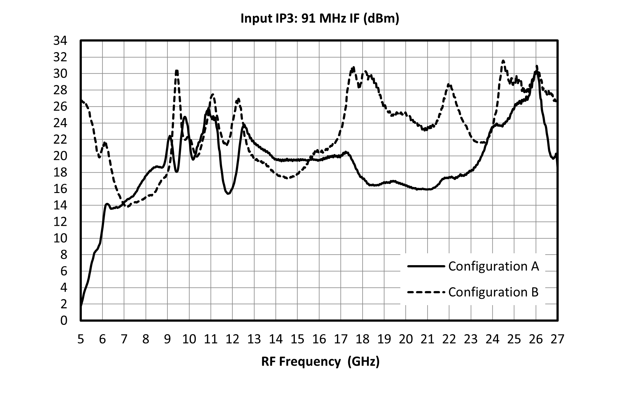
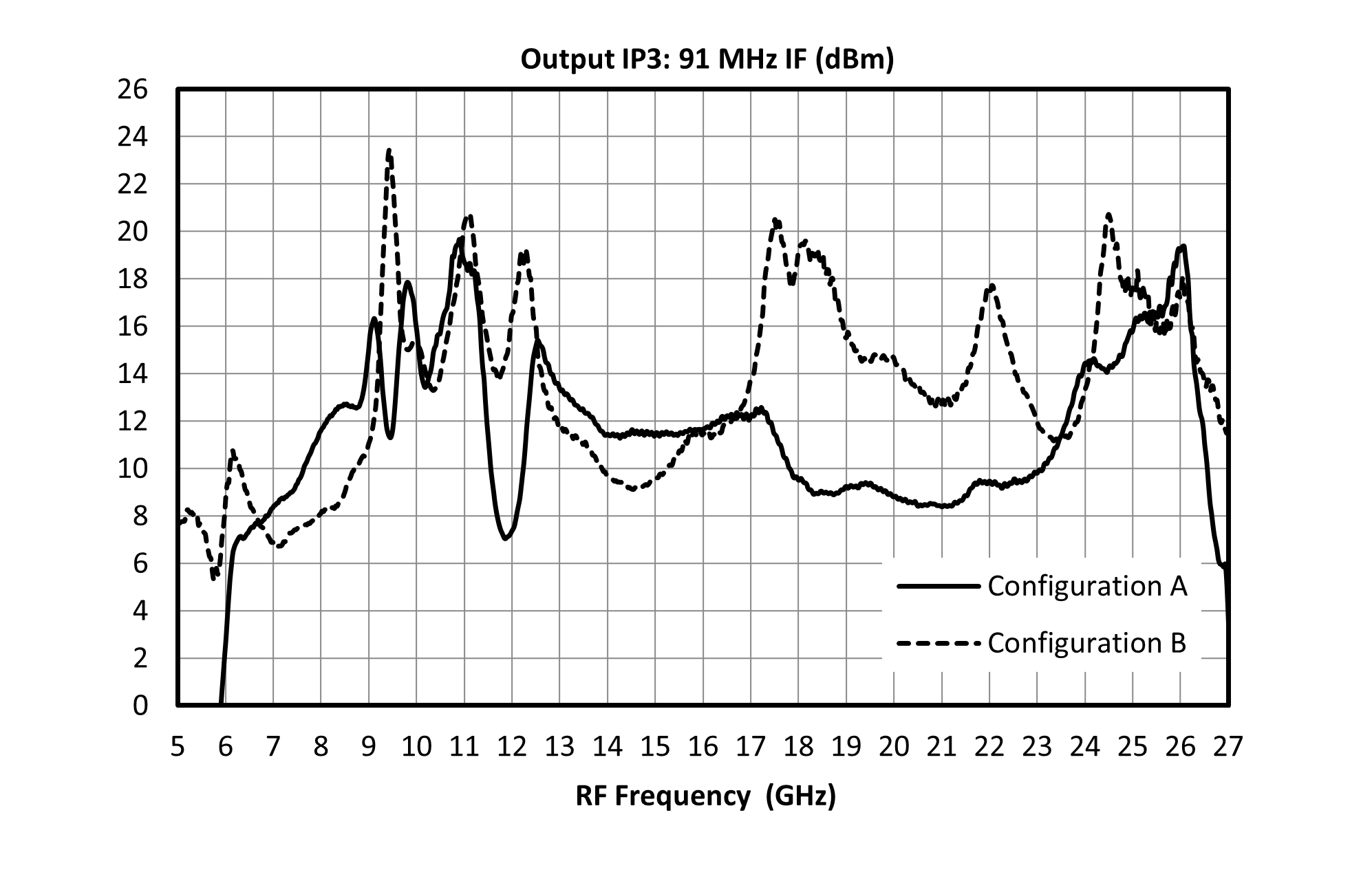
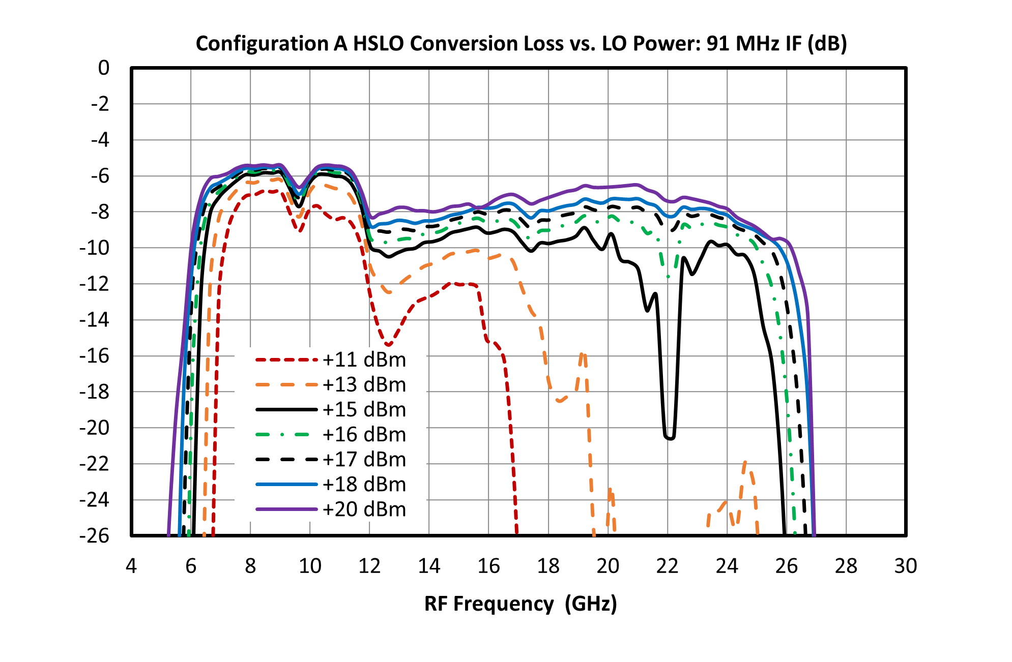
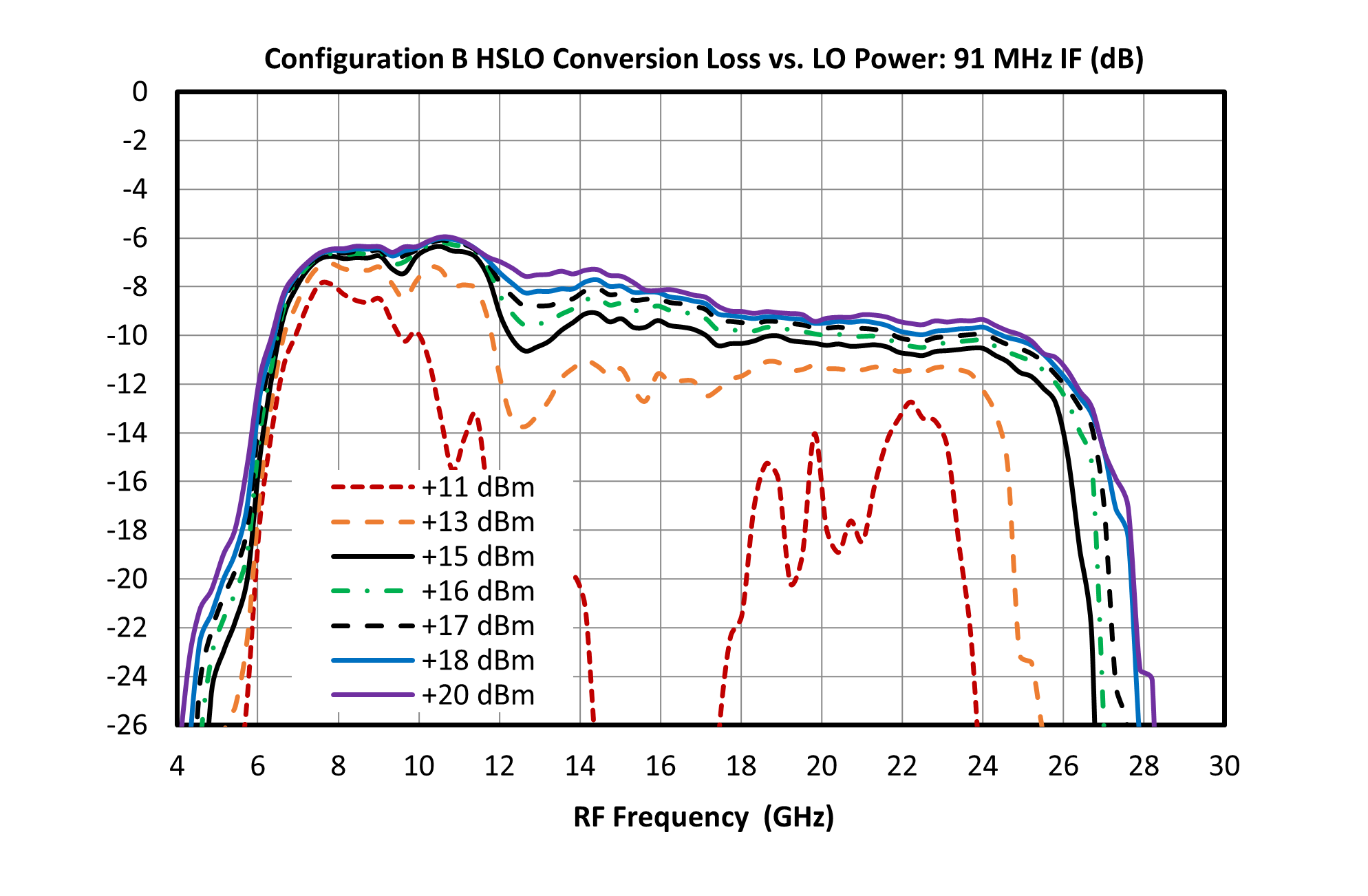
A bottom-up view of the MM1-0626HCSP2's CSP2 package outline drawing is shown below. The MM1-0626HCSP2 has the input and output ports given in Port Functions. The MM1-0626HCSP2 can be used in either an up or down conversion application. For configuration A, input the LO into pin 1, use pin 3 for the RF, and pin 2 for the IF. For configuration B, input the LO into pin 3, use pin 1 for the RF, and pin 2 for the IF.

Diagram of the port configuration for MM1-0626HCSP2

Port Functions

Configuration A

PortFunctionDescriptionDC Equivalent
Circuit
Pin 1LO Pin 1 is DC open and AC matched to 50 Ohms from 6 to 26.5 GHz. Blocking capacitor is optional.Equivalent circuit for the LO
Pin 2IF Pin 2 is DC coupled to the diodes. Blocking capacitor is optional.Equivalent circuit for the IF
Pin 3RF Pin 3 is DC open and AC matched to 50 Ohms from 6 to 26.5 GHz. Blocking capacitor is optional.Equivalent circuit for the RF
Pin 4,5N/C Pins 4 and 5 are not internally connected to the circuit and should be connected to GND.-

Rev: A | Copyright © 2024 - 2025 Marki Microwave LLC.

3

Configuration B

PortFunctionDescriptionDC Equivalent
Circuit
Pin 1RF Pin 1 is DC open and AC matched to 50 Ohms from 6 to 26.5 GHz. Blocking capacitor is optional.Equivalent circuit for the RF
Pin 2IF Pin 2 is DC coupled to the diodes. Blocking capacitor is optional.Equivalent circuit for the IF
Pin 3LO Pin 3 is DC open and AC matched to 50 Ohms from 6 to 26.5 GHz. Blocking capacitor is optional.Equivalent circuit for the LO
Pin 4,5N/C Pins 4 and 5 are not internally connected to the circuit and should be connected to GND.-

Rev: A | Copyright © 2024 - 2025 Marki Microwave LLC.

4

Specifications

Absolute Maximum Ratings

The Absolute Maximum Ratings indicate limits beyond which damage may occur to the device. If these limits are exceeded, the device may be inoperable or have a reduced lifetime.

ParameterMaximum RatingUnit
Maximum Operating Temperature 100°C
Maximum Storage Temperature 125°C
Minimum Operating Temperature -55°C
Minimum Storage Temperature -65°C
Port 2 DC Current 15mA
RF Power Handling (RF+LO), 100°C 21dBm
RF Power Handling (RF+LO), 25°C 25dBm

Package Information

ParameterDetailsRating
ESD250 to < 500 VoltsHBM Class 1A
Dimensions-2.50 x 2.50 mm
Moisture Sensitivity Level-MSL 1

The Recommended Operating Conditions indicate the limits, inside which the device should be operated, to guarantee the performance given in Electrical Specifications Operating outside these limits may not necessarily cause damage to the device, but the performance may degrade outside the limits of the electrical specifications. For limits, above which damage may occur, see Absolute Maximum Ratings.

ParameterMinNominalMaxUnit
LO Input Power 111520-

Rev: A | Copyright © 2024 - 2025 Marki Microwave LLC.

5

Electrical Specifications

The electrical specifications apply at TA=+25°C in a 50Ω system. Typical data shown is for a down conversion application with a +15 dBm sine wave LO input.

ParameterPort ConfigurationTest ConditionsMinTypMaxUnit
Conversion Loss 1ALO=6-26GHz
RF=6-26.5GHz
IF=DC-9GHz
LO drive level=15dBm
-7-dB
Input IP3 ALO=6-26GHz
RF=6-26.5GHz
IF=DC-9GHz
LO drive level=15dBm
-19.5-dBm
Input P1dB ALO=6-26.5GHz
RF=6-26GHz
IF=DC-9GHz
LO drive level=17-23dBm
-14-dB
LO-IF Isolation 2ALO=6-26GHz
RF=6-26.5GHz
IF=DC-9GHz
LO drive level=15dBm
-37-dB
LO-RF Isolation 3ALO=6-26GHz
RF=6-26.5GHz
IF=DC-9GHz
LO drive level=15dBm
-45-dB
Noise Figure 4ALO=6-26GHz
RF=6-26.5GHz
IF=DC-9GHz
LO drive level=15dBm
-7-dB
RF-IF Isolation 5ALO=6-26GHz
RF=6-26.5GHz
IF=DC-9GHz
LO drive level=15dBm
-42-dB
Conversion Loss 6BLO=6-26GHz
RF=6-26.5GHz
IF=DC-9GHz
LO drive level=15dBm
-8-dB
Input IP3 BLO=6-26GHz
RF=6-26.5GHz
IF=DC-9GHz
LO drive level=15dBm
-22.5-dBm
Input P1dB BLO=6-26GHz
RF=6-26.5GHz
IF=DC-9GHz
LO drive level=15dBm
-11-dBm
LO-IF Isolation 7BLO=6-26GHz
RF=6-26.5GHz
IF=DC-9GHz
LO drive level=15dBm
-42-dB
LO-RF Isolation 8BLO=6-26GHz
RF=6-26.5GHz
IF=DC-9GHz
LO drive level=15dBm
-45-dB
Noise Figure 9BLO=6-26GHz
RF=6-26.5GHz
IF=DC-9GHz
LO drive level=15dBm
-8-dB
RF-IF Isolation 10BLO=6-26GHz
RF=6-26.5GHz
IF=DC-9GHz
LO drive level=15dBm
-37-dB
IF Frequency Range --0-9GHz
LO Frequency Range --6-26GHz
RF Frequency Range --6-26GHz

[1][6] Measured as a down converter to a fixed 91MHz IF. Eval board IF and RF traces were de-embedded and LO trace power correction was applied.

[2][3][5][7][8][10] Eval board IF and RF traces were de-embedded and LO trace power correction was applied

[4][9] Mixer Noise Figure typically measures within 0.5dB of conversion loss for IF frequencies greater than 5 MHz.

Rev: A | Copyright © 2024 - 2025 Marki Microwave LLC.

6

Typical Performance

Conversion Loss: 91 MHz IF, HSLO (dB) graph for MM1-0626HCSP2
RF Return Loss (dB) graph for MM1-0626HCSP2
Relative IF Response (7GHz RF) graph for MM1-0626HCSP2
IF Return Loss (7GHz RF) graph for MM1-0626HCSP2
Relative IF Response (24GHz RF) graph for MM1-0626HCSP2
IF Return Loss, LSLO, 25GHz RF (dB) graph for MM1-0626HCSP2
LO to RF Isolation (dB) graph for MM1-0626HCSP2
LO Return Loss (dB) graph for MM1-0626HCSP2

Rev: A | Copyright © 2024 - 2025 Marki Microwave LLC.

7

LO to IF Isolation (dB) graph for MM1-0626HCSP2
RF to IF Isolation (dB) graph for MM1-0626HCSP2
Input IP3 vs Frequency graph for MM1-0626HCSP2
Output IP3 (dBm) graph for MM1-0626HCSP2
Configuration A Conversion Loss vs. LO Power: 91 MHz IF (dB) graph for MM1-0626HCSP2
Configuration B Conversion Loss vs. LO Power: 91 MHz IF (dB) graph for MM1-0626HCSP2
Even LO Harmonic to RF Isolation (dB) graph for MM1-0626HCSP2
Even LO Harmonic to IF Isolation (dB) graph for MM1-0626HCSP2

Rev: A | Copyright © 2024 - 2025 Marki Microwave LLC.

8

Odd LO Harmonic to RF Isolation (dB) graph for MM1-0626HCSP2
Odd LO Harmonic to IF Isolation (dB) graph for MM1-0626HCSP2
2RF x 2LO Spurious Suppression (dBc) graph for MM1-0626HCSP2
2IF x 1LO Spurious Suppression (dBc) -10 dBm IF input graph for MM1-0626HCSP2

Rev: A | Copyright © 2024 - 2025 Marki Microwave LLC.

9

Application Circuit

Application Circuit for MM1-0626HCSP2

Rev: A | Copyright © 2024 - 2025 Marki Microwave LLC.

10

Mechanical Data

Rev: A | Copyright © 2024 - 2025 Marki Microwave LLC.

11

Rev: A | Copyright © 2024 - 2025 Marki Microwave LLC.

12