Port Diagram
Sales: 408-778-9952 | General: 408-778-4200 | Fax: 408-778-4300
Sales & Customer Support: [email protected]
Tech Support: [email protected]
The MM1-0424S is a high linearity passive double balanced MMIC mixer. The S diode offers superior 1 dB compression, two tone intermodulation performance, and spurious suppression, compared to other GaAs MMIC mixers. It features excellent conversion loss, superior isolations and spurious performance across a broad bandwidth, in a miniature form factor. The MM1-0424SSM is available in a lead-free, RoHS compliant QFN surface mount package and is compatible with standard leaded and lead-free PCB reflow soldering processes. The MM1-0424SSM is a superior alternative to Marki Microwave surface mount M1 and M3 mixers.
N/A

| Part Number | Description | Package | Packing Size | Green Status | Product Lifecycle | Export Classification |
|---|---|---|---|---|---|---|
| MM1-0424SSM-2 | GaAs Double-Balanced Mixer | QFN | - | REACH RoHS | Released | EAR99 |
| EVAL-MM1-0424S | Evaluation Board, GaAs DOUBLE-BALANCED MIXER | EVAL | - | REACH RoHS | Released | EAR99 |
| MM1-0424S-2-TR | Tape and Reel, GaAs Double-Balanced Mixer | QFN | 7" | REACH RoHS | Released | EAR99 |
MM1-0424SSM-2
GaAs Double-Balanced Mixer
| Revision Code | Revision Date | Comment |
|---|---|---|
| - | 2016-08-01 | Initial Release |
| A | 2019-04-01 | Updated plating to ENEPIG |
| B | 2025-08-22 | ESD Class added |
MM1-0424SSM-2
GaAs Double-Balanced Mixer
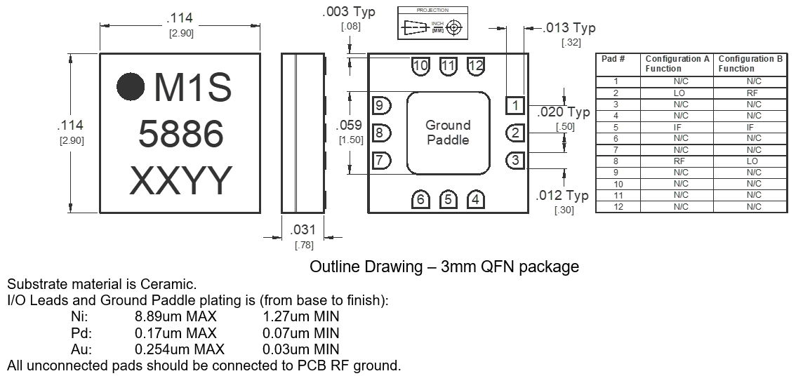
| Port | Function | Description | DC Equivalent Circuit |
|---|---|---|---|
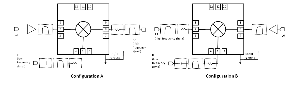
| Port 2 | LO | Port 2 is DC short to ground and AC matched to 50 Ohms from 4.5 to 24 GHz. Blocking capacitor is optional. |  |
| Port 5 | IF | Port 5 is DC coupled to the diodes. Blocking capacitor is optional. |  |
| Port 8 | RF | Port 8 is DC short to ground and AC matched to 50 Ohms from 4.5 to 24 GHz. Blocking capacitor is optional. | |
MM1-0424SSM-2
GaAs Double-Balanced Mixer
| Port | Function | Description | DC Equivalent Circuit |
|---|---|---|---|
| Port 2 | RF | Port 2 is DC short to ground and AC matched to 50 Ohms from 4.5 to 24 GHz. Blocking capacitor is optional. | |
| Port 5 | IF | Port 5 is DC coupled to the diodes. Blocking capacitor is optional. | |
| Port 8 | LO | Port 8 is DC short to ground and AC matched to 50 Ohms from 4.5 to 24 GHz. Blocking capacitor is optional. | |
MM1-0424SSM-2
GaAs Double-Balanced Mixer
| Parameter | Maximum Rating | Unit |
|---|---|---|
| Maximum Operating Temperature | 100 | °C |
| Maximum Storage Temperature | 125 | °C |
| Minimum Operating Temperature | -55 | °C |
| Minimum Storage Temperature | -65 | °C |
| Port 2 DC Current | 15 | mA |
| Port 5 DC Current | 30 | mA |
| Port 8 DC Current | 15 | mA |
| RF Power Handling (RF+LO), 100°C | 24 | dBm |
| RF Power Handling (RF+LO), 25°C | 28 | dBm |
| Parameter | Details | Rating |
|---|---|---|
| ESD | 250 to < 500 Volts | HBM Class 1A |
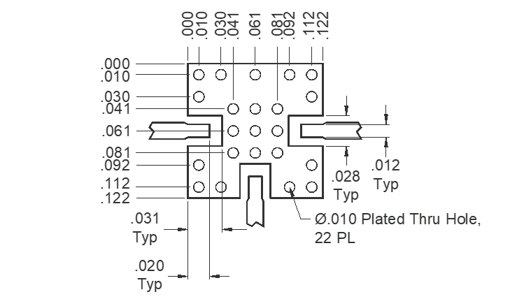
| Dimensions | - | 3 x 3 mm |
| Moisture Sensitivity Level | - | MSL 1 |
| Parameter | Min | Nominal | Max | Unit |
|---|---|---|---|---|
| LO Input Power | 17 | - | 23 | - |
MM1-0424SSM-2
GaAs Double-Balanced Mixer
Specifications guaranteed from -55 to +100°C, measured in a 50Ω system. Specifications are shown for Configurations A & B.
| Parameter | Port Configuration | Test Conditions | Min | Typ | Max | Unit |
|---|---|---|---|---|---|---|
| Conversion Loss | A | LO/RF=4.5-24 GHz IF=DC-4 GHz | - | 8 | 13 | dB |
| IF Frequency Range | A | - | 0 | - | 4 | GHz |
| Input IP3 | A | A: LO/RF=4.5-24 GHz IF=DC-4 GHz LO Drive Level= 18-23 | - | 25 | - | dBm |
| Input P1dB | A | LO/RF=4.5-24 GHz IF=DC-4 GHz LO Drive Level= 18-23 | - | 14 | - | dBm |
| LO Frequency Range | A | - | 4.5 | - | 24 | GHz |
| RF Frequency Range | A | - | 4.5 | - | 24 | GHz |
| Conversion Loss | B | LO/RF=4.5-24 GHz IF=DC-4 GHz | - | 9 | 16 | dB |
| Input IP3 | B | B: LO/RF=4.5-24 GHz IF=DC-4 GHz LO Drive Level= 17-23 | - | 23 | - | dBm |
| Input P1dB | B | B: LO/RF=4.5-24 GHz IF=DC-4 GHz LO Drive Level= 17-23 | - | 14 | - | dBm |
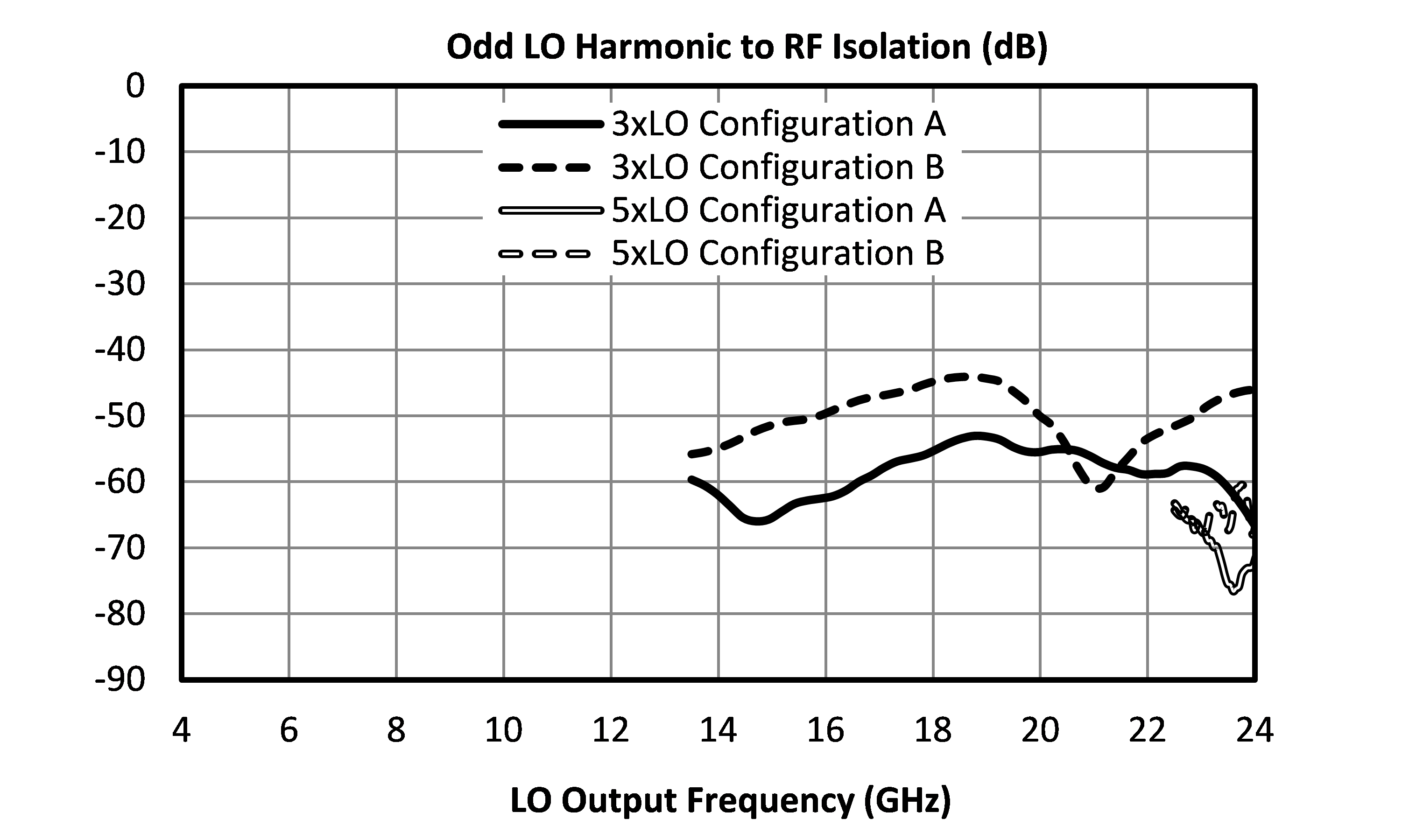
| LO-RF Isolation | - | - | - | 48 | - | dB |
| Parameter | Port Configuration | Test Conditions | Min | Typ | Max | Unit |
|---|---|---|---|---|---|---|
| Conversion Loss | A | LO/RF=4.5-24 GHz IF=DC-4 GHz | - | 8 | 13 | dB |
| IF Frequency Range | A | - | 0 | - | 4 | GHz |
| Input IP3 | A | A: LO/RF=4.5-24 GHz IF=DC-4 GHz LO Drive Level= 18-23 | - | 25 | - | dBm |
| Input P1dB | A | LO/RF=4.5-24 GHz IF=DC-4 GHz LO Drive Level= 18-23 | - | 14 | - | dBm |
| LO Frequency Range | A | - | 4.5 | - | 24 | GHz |
| RF Frequency Range | A | - | 4.5 | - | 24 | GHz |
| Conversion Loss | B | LO/RF=4.5-24 GHz IF=DC-4 GHz | - | 9 | 16 | dB |
| Input IP3 | B | B: LO/RF=4.5-24 GHz IF=DC-4 GHz LO Drive Level= 17-23 | - | 23 | - | dBm |
| Input P1dB | B | B: LO/RF=4.5-24 GHz IF=DC-4 GHz LO Drive Level= 17-23 | - | 14 | - | dBm |
| LO-RF Isolation | - | - | - | 48 | - | dB |
MM1-0424SSM-2
GaAs Double-Balanced Mixer


MM1-0424SSM-2
GaAs Double-Balanced Mixer


MM1-0424SSM-2
GaAs Double-Balanced Mixer


MM1-0424SSM-2
GaAs Double-Balanced Mixer
MM1-0424SSM-2
GaAs Double-Balanced Mixer
MM1-0424SSM-2
GaAs Double-Balanced Mixer