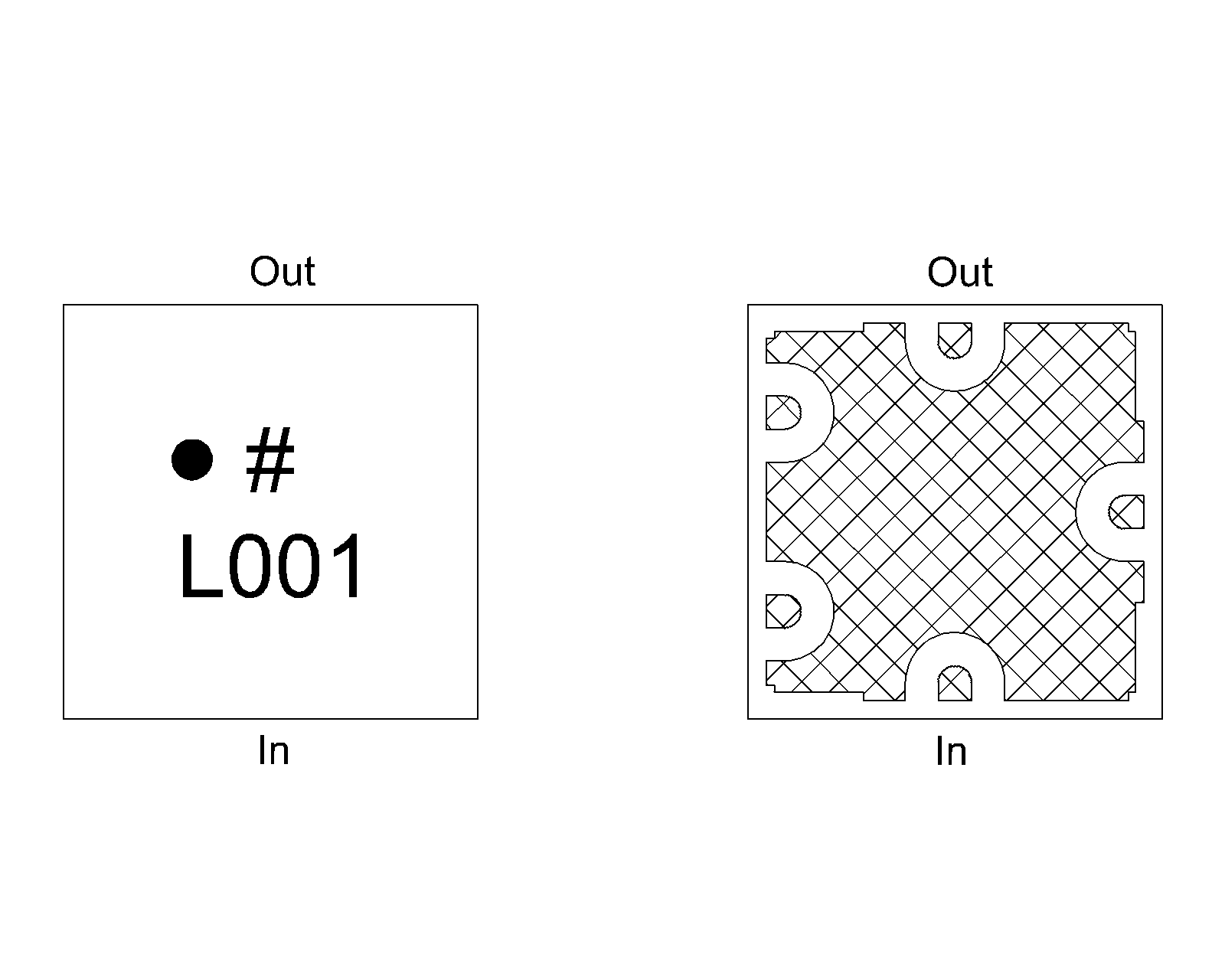
Port Diagram
A top-down view of the HLM-70CPS2’s CSP2 package outline drawing is shown below. The HLM-70CSP2 has the input and output ports given in Port Functions.
Sales: 408-778-9952 | General: 408-778-4200 | Fax: 408-778-4300
Sales & Customer Support: [email protected]
Tech Support: [email protected]
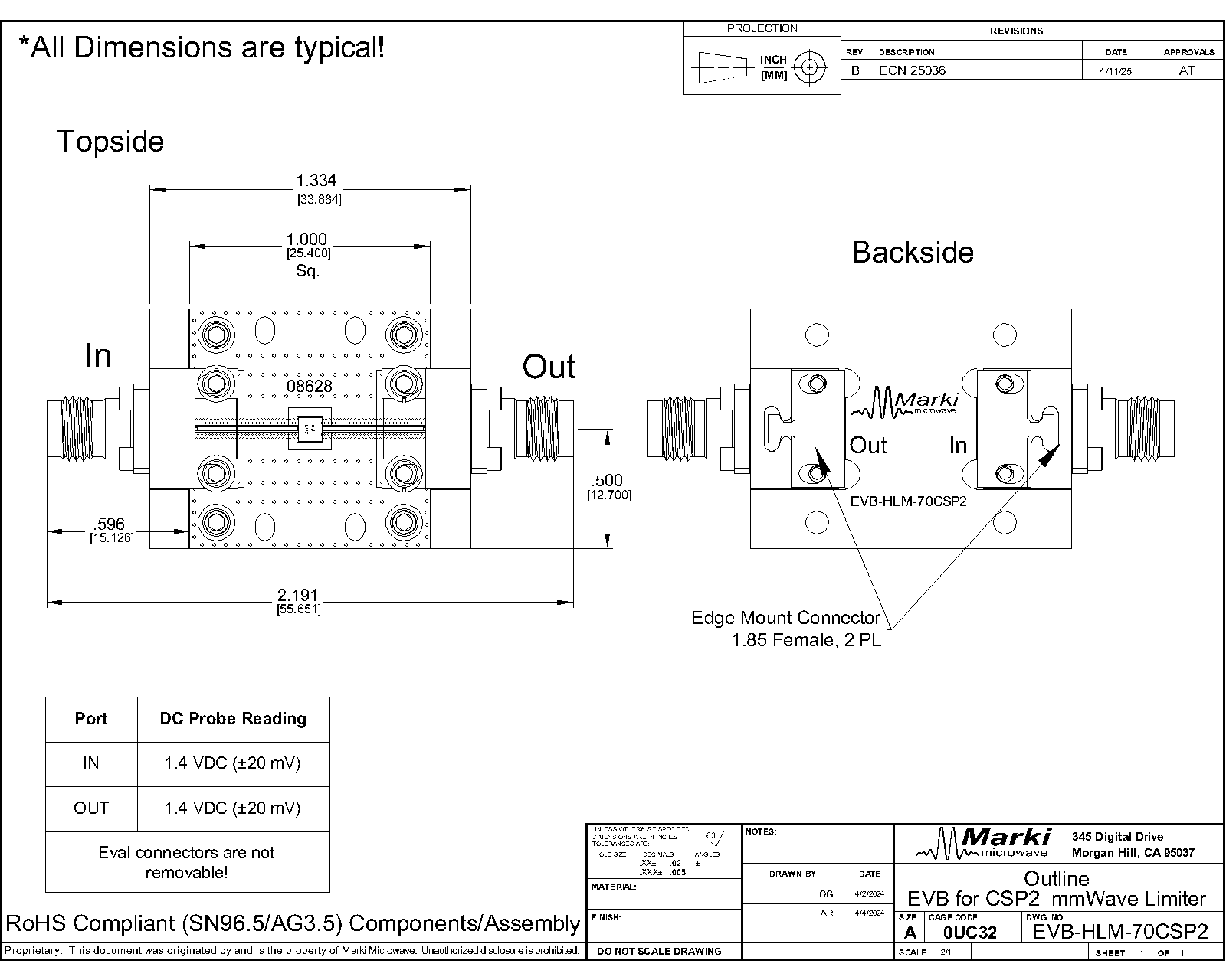
The HLM-70CSP2 is a high-linearity GaAs Schottky diode signal limiter featuring high IP3 over a broad DC - 70GHz bandwidth. It offers low insertion loss and excellent return loss over a wide operating bandwidth. Its small size makes it ideal for protecting sensitive components and for applications requiring high channel counts. It is available as a plastic surface mount chip scale package or as a connectorized evaluation board.

N/A

| Part Number | Description | Package | Green Status | Product Lifecycle | Export Classification |
|---|---|---|---|---|---|
| HLM-70CSP2 | DC - 70GHz Chip Scale Package Limiter | CSP2 | REACH RoHS | Released | EAR99 |
| EVB-HLM-70CSP2 | DC - 70 GHz Chip Scale Package Limiter | EVB | Released | EAR99 |
HLM-70CSP2
DC - 70GHz Chip Scale Package Limiter
| Revision Code | Revision Date | Comment |
|---|---|---|
| - | 2024-06-03 | Initial Release |
| A | 2025-04-28 | Updated Moisture Sensitivity from MSL3 to MSL1 |
| B | 2025-05-05 | Added ESD rating |
| C | 2026-06-02 | Added Recovery Time and Spike Leakage |
HLM-70CSP2
DC - 70GHz Chip Scale Package Limiter
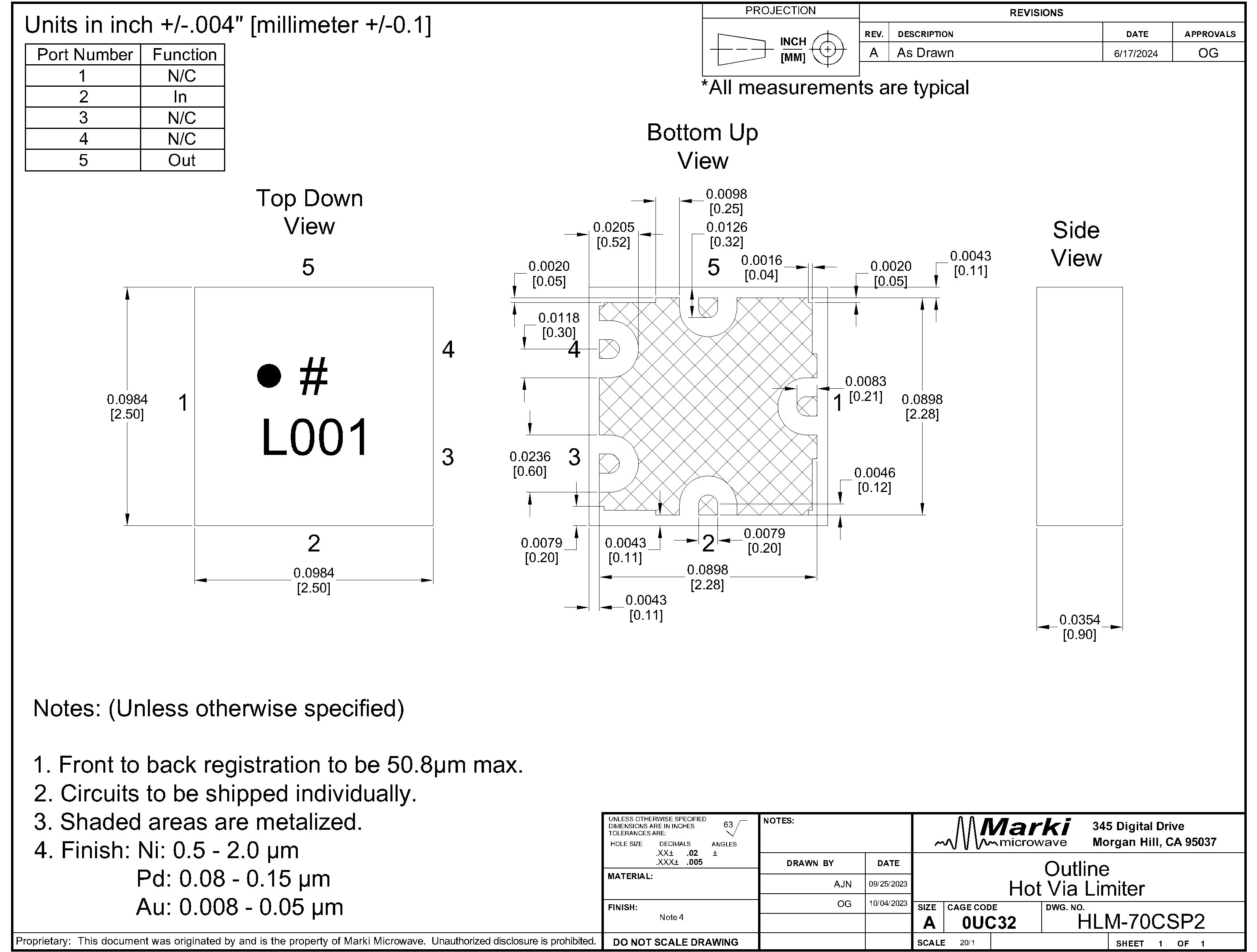
A top-down view of the HLM-70CPS2’s CSP2 package outline drawing is shown below. The HLM-70CSP2 has the input and output ports given in Port Functions.
| Port | Function | Description | DC Equivalent Circuit |
|---|---|---|---|
| Ground Paddle | Ground | CSP2 package ground path is provided through the ground paddle and should be connected to RF ground |  |
| IN | Input | The input port is diode connected for the CSP2 and EVAL package. |  |
| Output | Output | The output port is diode connected for the CSP2 and EVAL package. |  |
HLM-70CSP2
DC - 70GHz Chip Scale Package Limiter
The Absolute Maximum Ratings indicate limits beyond which damage may occur to the device. If these limits are exceeded, the device may be inoperable or have a reduced lifetime.
| Parameter | Maximum Rating | Unit |
|---|---|---|
| Maximum Operating Temperature | 100 | °C |
| Maximum Storage Temperature | 125 | °C |
| Minimum Operating Temperature | -55 | °C |
| Minimum Storage Temperature | -65 | °C |
| RF Power Handling , Average | 1 | W |
| Parameter | Details | Rating |
|---|---|---|
| ESD | 250 to < 500 Volts | HBM Class 1A |
| Dimensions | - | 2.50 x 2.50 mm |
| Moisture Sensitivity Level | - | MSL 1 |
HLM-70CSP2
DC - 70GHz Chip Scale Package Limiter
The electrical specifications apply at TA=+25°C in a 50Ω system. Typical data shown is for the connectorized EVAL-package limiter unless otherwise specified. CSP1-package data shown is deembedded from the EVAL-package data. Linear Specifications valid for input power up to the 0.1dB compression point. See page 5 for P0.1dB graph. Min and Max limits are guaranteed at TA=+25°C.
| Parameter | Test Conditions | Minimum Frequency (GHz) | Maximum Frequency (GHz) | Min | Typ | Max | Unit |
|---|---|---|---|---|---|---|---|
| Spike Leakage | - | - | - | - | 0.1 | - | erg |
| Recovery Time | - | - | - | - | 8 | - | ns |
| Flat Leakage | 18 GHz CW | - | - | - | 18 | - | dBm |
| Flat Leakage | 20GHz CW | - | - | - | 17 | - | dBm |
| Flat Leakage | 40GHz CW | - | - | - | 13 | - | dBm |
| Input IP3 | DC – 60GHz | 0 | 70 | - | 32 | - | dBm |
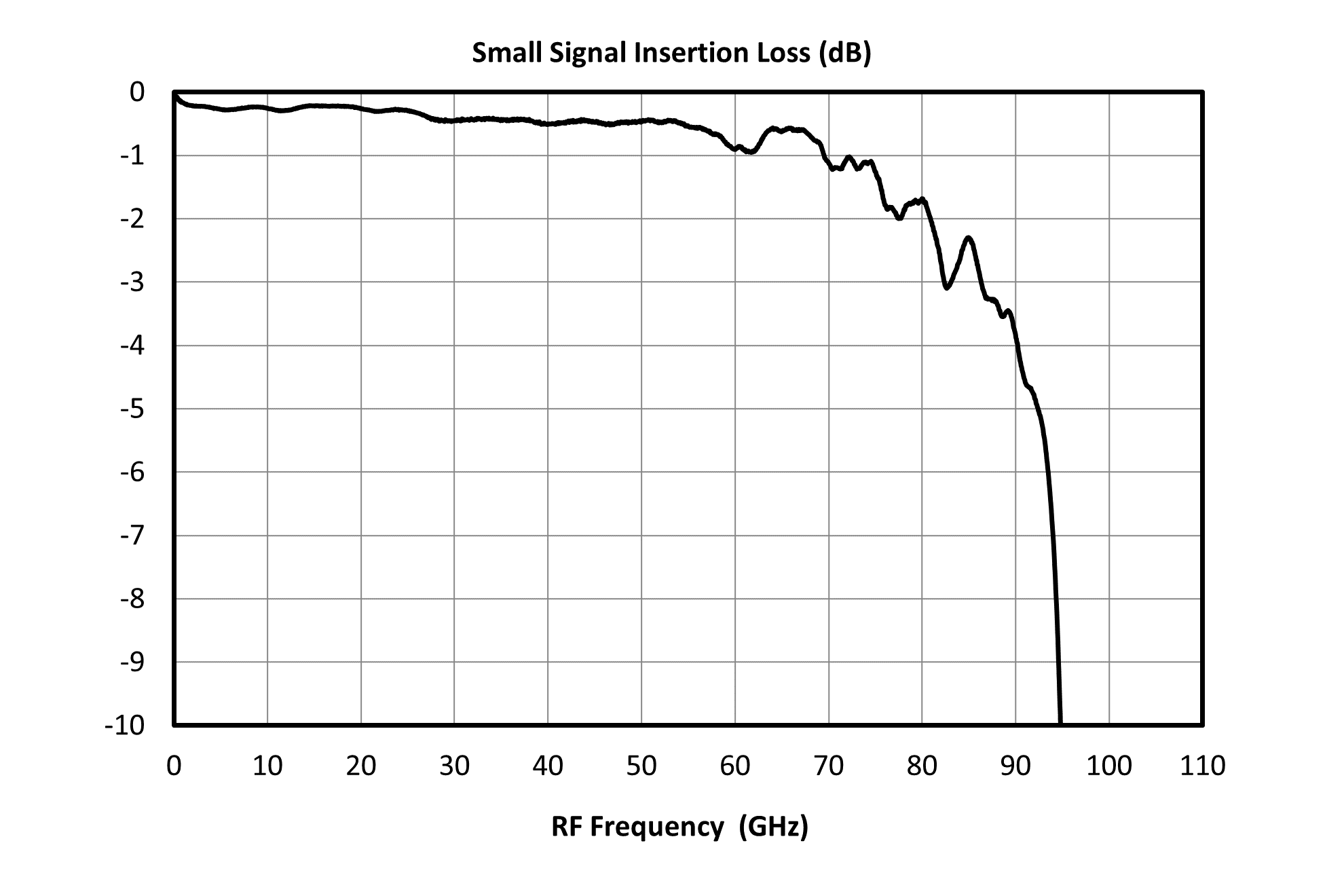
| Insertion Loss | DC – 70GHz | 0 | 70 | - | 0.5 | - | dB |
| Return Loss | DC – 70GHz | 0 | 70 | - | 21 | - | dB |
| Parameter | Test Conditions | Minimum Frequency (GHz) | Maximum Frequency (GHz) | Min | Typ | Max | Unit |
|---|---|---|---|---|---|---|---|
| Spike Leakage | - | - | - | - | 0.1 | - | erg |
| Recovery Time | - | - | - | - | 8 | - | ns |
| Flat Leakage | 18 GHz CW | - | - | - | 18 | - | dBm |
| Flat Leakage | 20GHz CW | - | - | - | 17 | - | dBm |
| Flat Leakage | 40GHz CW | - | - | - | 13 | - | dBm |
| Input IP3 | DC – 60GHz | 0 | 70 | - | 32 | - | dBm |
| Insertion Loss | DC – 70GHz | 0 | 70 | - | 0.5 | - | dB |
| Return Loss | DC – 70GHz | 0 | 70 | - | 21 | - | dB |
HLM-70CSP2
DC - 70GHz Chip Scale Package Limiter


HLM-70CSP2
DC - 70GHz Chip Scale Package Limiter


.png)


HLM-70CSP2
DC - 70GHz Chip Scale Package Limiter


HLM-70CSP2
DC - 70GHz Chip Scale Package Limiter
HLM-70CSP2
DC - 70GHz Chip Scale Package Limiter
Download : Footprint Drawing

HLM-70CSP2
DC - 70GHz Chip Scale Package Limiter