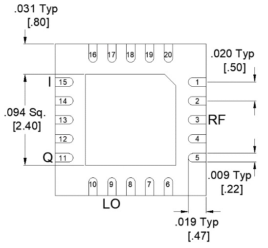
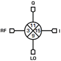
Device Overview

General Description

The MMIQ-1867LSM is a low LO drive, passive GaAs MMIC IQ mixer. This is an ultra-broadband mixer spanning 18 to 67 GHz on the RF and LO ports with an IF from DC to 23 GHz. Up to 50 dB of image rejection is available due to the excellent phase and amplitude balance of its on-chip LO quadrature hybrid. Both surface QFNs and evaluation boards are available.

Photo of MMIQ-1867LSM-2

Features

RF/LO Frequency Range: 18 - 67 GHz
IF Frequency Range: DC - 23 GHz
I+Q Conversion Loss: 9 dB
Image Rejection: 32 dB
LO-RF Isolation: 49 dB

Applications

  • Single Sideband and Image Rejection Mixing
  • IQ Modulation / Demodulation
  • Vector Amplitude Modulation
  • Band Shifting
  • 5G Band Support

Functional Block Diagram

Block Diagram

Part Ordering Options

Part NumberDescriptionPackageGreen StatusProduct LifecycleExport Classification
MMIQ-1867LSM-2Low LO Drive Surface Mount MMIC IQ MixerQFN

REACH

RoHS

ReleasedEAR99
EVAL-MMIQ-1867LEvaluation Board, Low LO Drive Surface Mount MMIC 18-67 GHz IQ MixerEVAL

REACH

RoHS

ReleasedEAR99

Table Of Contents

Revision History

Revision CodeRevision DateComment
-2020-12-01Datasheet Initial Release

Rev: - | Copyright © 2020 Marki Microwave LLC.

2

Port Configuration and Functions

Port Diagram

A bottom-up view of the MMIQ-1867LSM’s SMT package outline drawing is shown below. The mixer may be operated as either a downconverter or an upconverter. Use of the RF or IF as the input or output port will depend on the application. See Application Information for input and output port configuration for common applications.

Diagram of the port configuration for MMIQ-1867LSM-2

Port Functions

PortFunctionDescriptionDC Equivalent
Circuit
GNDGround SM package ground path is provided through the ground paddle.Equivalent circuit for the Ground
Pin 11Q Input / Output Port 11 is diode coupled and AC matched to 50Ω over the specified Q port frequency range.Equivalent circuit for the Q Input / Output
Pin 15I Input / Output Port 15 is diode coupled and AC matched to 50Ω over the specified I port frequency range.Equivalent circuit for the I Input / Output
Pin 3RF Input / Output Port 3 is DC open and AC matched to 50Ω over the specified RF frequency range.Equivalent circuit for the RF Input / Output
Pin 9LO Input Port 9 is DC open and AC matched to 50Ω over the specified LO frequency range. Equivalent circuit for the LO Input

Rev: - | Copyright © 2020 Marki Microwave LLC.

3

Specifications

Absolute Maximum Ratings

The Absolute Maximum Ratings indicate limits beyond which damage may occur to the device. If these limits are exceeded, the device may be inoperable or have a reduced lifetime.

ParameterMaximum RatingUnit
Maximum Operating Temperature 100°C
Maximum Storage Temperature 125°C
Minimum Operating Temperature -55°C
Minimum Storage Temperature -65°C
Pin 11 DC Current 30mA
Pin 15 DC Current 30mA
Power Handling, at any Port 26dBm

Package Information

ParameterDetailsRating
ESD250 to < 500 VoltsHBM Class 1A
Dimensions-4 x 4 mm
Moisture Sensitivity Level-MSL 1

The Recommended Operating Conditions indicate the limits, inside which the device should be operated, to guarantee the performance given in Electrical Specifications. Operating outside these limits may not necessarily cause damage to the device, but the performance may degrade outside the limits of the electrical specifications. For limits, above which damage may occur, see Absolute Maximum Ratings.

ParameterMinNominalMaxUnit
Ambient Temperature -5525100°C
RF/IF Input Power --3dBm
LO Input Power 81319dBm

Rev: - | Copyright © 2020 Marki Microwave LLC.

4

Electrical Specifications

The electrical specifications apply at TA=+25°C in a 50Ω system. Typical data shown is for a down conversion application with a +13 dBm sine wave LO input. Min and Max limits apply only to our connectorized units and are guaranteed at TA=+25°C.

ParameterTest ConditionsMinimum
Frequency
(GHz)
Maximum
Frequency
(GHz)
MinTypMaxUnit
Amplitude Balance -- --0.2-dB
Conversion Loss 1RF/LO = 18 - 67 GHz
I = 0.2 - 23 GHz
18 67-16-dB
Conversion Loss 2RF/LO = 18 - 67 GHz
I = DC - 0.2 GHz
18 67-1218dB
Conversion Loss 3RF/LO = 18 - 67 GHz
I+Q = 0.2 - 23 GHz
18 67-13-dB
Conversion Loss 4RF/LO = 18 - 67 GHz
I+Q = DC - 0.2 GHz
18 67-9-dB
Conversion Loss 5RF/LO = 18 - 67 GHz
Q = 0.2 - 23 GHz
18 67-16-dB
Conversion Loss 6RF/LO = 18 - 67 GHz
Q = DC - 0.2 GHz
18 67-1219dB
IF Frequency Range -- -0-23GHz
Image Rejection 7RF/LO = 18 - 67 GHz
I+Q = DC – 0.2 GHz
18 67-32-dBc
Input 1 dB Gain Compression Point (P1dB), I -- --4.5-dBm
Input 1 dB Gain Compression Point (P1dB), Q -- --3.5-dBm
Input IP3 8RF/LO = 18 - 67 GHz
I = DC – 0.2 GHz
18 67-16.5-dBm
Isolation, LO to I IF/LO = 18 - 67 GHz
18 67-43-dB
Isolation, LO to Q IF/LO = 18 - 67 GHz
18 67-55-dB
Isolation, RF to I RF/IF = 18 - 67 GHz
18 67-55-dB
Isolation, RF to Q RF/IF = 18 - 67 GHz
18 67-55-dB
LO Frequency Range -- -18-67GHz
LO-RF Isolation RF/LO = 18 - 67 GHz
18 67-48.5-dB
Noise Figure 9RF/LO = 18 - 67 GHz
I = DC – 0.2 GHz
18 67-12-dB
Noise Figure 10RF/LO = 18 - 67 GHz
Q = DC – 0.2 GHz
18 67-12-dB
Phase Balance -- --3-°
Q (Pin 11) Frequency Range -- -0-23GHz
RF Frequency Range -- -18-67GHz

[1][2][3][4][5][6] Measured as an I/Q down converter (i.e., I and Q powers are not combined)

[7] Image Rejection and Single sideband performance plots are defined by the upper sideband (USB) or lower sideband (LSB) with respect to the LO signal. Plots are defined by which sideband is selected by the external IF quadrature hybrid.

[8] Typical IIP3 is measured with I and Q ports combined with an external quadrature hybrid coupler in a down conversion.

[9][10] Mixer Noise Figure typically measures within 0.5 dB of conversion loss for IF frequencies greater than 5 MHz.

Rev: - | Copyright © 2020 Marki Microwave LLC.

5

Typical Performance Plots

I output means that the IF output signal is measured at the I port of the mixer and the Q port is loaded. Q output means the IF output signal is measured at the Q port of the mixer while the I port is loaded.

USB I+Q Downconversion Loss vs. LO Power (dB) graph for MMIQ-1867LSM-2
USB I+Q Downconversion Image Rejection vs. LO Power (dBc) graph for MMIQ-1867LSM-2
LSB I+Q Downconversion Loss vs. LO Power (dB) graph for MMIQ-1867LSM-2
LSB I+Q Downconversion Image Rejection vs. LO Power (dBc) graph for MMIQ-1867LSM-2
LO to RF Isolation (dB) graph for MMIQ-1867LSM-2
LO to IF Isolation (dB) graph for MMIQ-1867LSM-2

Rev: - | Copyright © 2020 Marki Microwave LLC.

6

RF to IF Isolation (dB) graph for MMIQ-1867LSM-2
RF Return Loss (dB) graph for MMIQ-1867LSM-2
LO Return Loss (dB) graph for MMIQ-1867LSM-2
IF Return Loss (dB) graph for MMIQ-1867LSM-2
Relative IF Response (dB) graph for MMIQ-1867LSM-2
I/Q Amplitude Balance vs. LO Power (dB) graph for MMIQ-1867LSM-2
I/Q Quadrature Phase Balance vs. LO Power (°) graph for MMIQ-1867LSM-2
USB I+Q Upconversion Loss vs. LO Power (dB) graph for MMIQ-1867LSM-2

Rev: - | Copyright © 2020 Marki Microwave LLC.

7

USB I+Q Upconversion Sideband Suppression (dBc) graph for MMIQ-1867LSM-2
LSB I+Q Upconversion Loss vs. LO Power (dB) graph for MMIQ-1867LSM-2
LSB I+Q Upconversion Sideband Suppression vs. LO Power (dBc) graph for MMIQ-1867LSM-2

Rev: - | Copyright © 2020 Marki Microwave LLC.

8

Typical Performance Plots: 6 GHz IF Downconversion Loss w/ AMM-7210SM LO Driver

Parameter 1

I+Q measurements taken with an external quadrature hybrid attached to the I and Q ports of the mixer. Orientation depends on up conversion or down conversion measurement.

MMIQ-1867LSM + AMM-7210SM: 6GHz IF Conversion Loss (dB) graph for MMIQ-1867LSM-2

Rev: - | Copyright © 2020 Marki Microwave LLC.

9

Typical Performance Plots: IP3

I+Q Input IP3 (dBm) graph for MMIQ-1867LSM-2
I+Q Output IP3 (dBm) graph for MMIQ-1867LSM-2
I+Q Input IP3 vs. LO Power (dBm) graph for MMIQ-1867LSM-2
I+Q Output IP3 vs. LO Power (dBm) graph for MMIQ-1867LSM-2

Rev: - | Copyright © 2020 Marki Microwave LLC.

10

Typical Performance Plots: LO Harmonic Isolation

Even LO Harmonic to RF Isolation (dB) graph for MMIQ-1867LSM-2
Even LO Harmonic to IF Isolation (dB) graph for MMIQ-1867LSM-2
Odd LO Harmonic to RF Isolation (dB) graph for MMIQ-1867LSM-2
Odd LO Harmonic to IF Isolation (dB) graph for MMIQ-1867LSM-2

Rev: - | Copyright © 2020 Marki Microwave LLC.

11

Application Circuit

Application Circuit for MMIQ-1867LSM-2

Rev: - | Copyright © 2020 Marki Microwave LLC.

12

Mechanical Data

Outline Drawing

Download : Outline 3D Drawing Outline 3D STP

Outline Drawing

Rev: - | Copyright © 2020 Marki Microwave LLC.

13

Footprint Image

Footprint of the package for MMIQ-1867LSM-2

Rev: - | Copyright © 2020 Marki Microwave LLC.

14

Evaluation Board - Outline Drawing

Outline Drawing

Rev: - | Copyright © 2020 Marki Microwave LLC.

15