Port Diagram
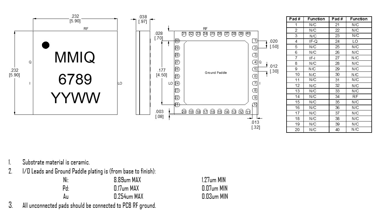
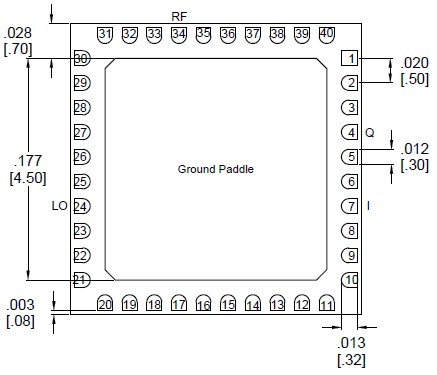
A bottom-up view of the MMIQ-0218L’s SM package outline drawing is shown below. The mixer may be operated as either a downconverter or an upconverter. Use of the RF or IF as the input or output port will depend on the application.
Sales: 408-778-9952 | General: 408-778-4200 | Fax: 408-778-4300
Sales & Customer Support: [email protected]
Tech Support: [email protected]
The MMIQ-0218LSM is a broadband passive GaAs MMIC IQ mixer that operates across an unrivaled 2-18 GHz RF/LO band with an IF from DC to 3 GHz. Excellent phase and amplitude balance of the on-chip LO quadrature hybrid leads to typical image rejection of 27 dB. Surface QFNs and evaluation boards are available.

N/A

| Part Number | Description | Package | Green Status | Product Lifecycle | Export Classification |
|---|---|---|---|---|---|
| MMIQ-0218LSM-2 | Broadband Drive Surface Mount MMIC IQ Mixer | QFN | REACH RoHS | Released | EAR99 |
| EVAL-MMIQ-0218L | Evaluation Board, Low LO Drive MMIC 2 - 18 GHz IQ Mixer | EVAL | REACH RoHS | Released | EAR99 |
MMIQ-0218LSM-2
Broadband Drive Surface Mount MMIC IQ Mixer
| Revision Code | Revision Date | Comment |
|---|---|---|
| - | 2020-01-01 | Initial Datasheet Release |
| A | 2020-05-01 | Added Vector Modulator Performance |
| B | 2020-06-01 | Added Spur Tables |
MMIQ-0218LSM-2
Broadband Drive Surface Mount MMIC IQ Mixer
A bottom-up view of the MMIQ-0218L’s SM package outline drawing is shown below. The mixer may be operated as either a downconverter or an upconverter. Use of the RF or IF as the input or output port will depend on the application.
| Port | Function | Description | DC Equivalent Circuit |
|---|---|---|---|
| GND | Ground | SM package ground path is provided through the ground paddle. |  |
| Pin 24 | LO Input | Pin 24 is DC short and AC matched to 50Ω over the specified LO frequency range. |  |
| Pin 34 | RF Input / Output | Pin 34 is DC short and AC matched to 50Ω over the specified RF frequency range. | |
| Pin 4 | Q Input / Output | Pin 4 is diode coupled and AC matched to 50Ω over the specified Q port frequency range. |  |
| Pin 7 | I Input / Output | Pin 7 is diode coupled and AC matched to 50Ω over the specified I port frequency range. | |
MMIQ-0218LSM-2
Broadband Drive Surface Mount MMIC IQ Mixer
The Absolute Maximum Ratings indicate limits beyond which damage may occur to the device. If these limits are exceeded, the device may be inoperable or have a reduced lifetime.
| Parameter | Maximum Rating | Unit |
|---|---|---|
| DC Current, any pin | 30 | mA |
| Maximum Operating Temperature | 100 | °C |
| Maximum Storage Temperature | 125 | °C |
| Minimum Operating Temperature | -55 | °C |
| Minimum Storage Temperature | -65 | °C |
| Power Handling, at any Port | 26 | dBm |
| Parameter | Details | Rating |
|---|---|---|
| ESD | 250 to < 500 Volts | HBM Class 1A |
| Weight | Package name: QFN | 0.1g |
| Dimensions | - | 6 x 6 mm |
| Moisture Sensitivity Level | - | MSL 1 |
The Recommended Operating Conditions indicate the limits, inside which the device should be operated, to guarantee the performance given in Electrical Specifications. Operating outside these limits may not necessarily cause damage to the device, but the performance may degrade outside the limits of the electrical specifications. For limits, above which damage may occur, see Absolute Maximum Ratings.
| Parameter | Min | Nominal | Max | Unit |
|---|---|---|---|---|
| Ambient Temperature | -55 | 25 | 100 | °C |
| RF/IF Input Power | - | - | 5 | dBm |
| LO Input Power | 14 | 17 | 20 | dBm |
MMIQ-0218LSM-2
Broadband Drive Surface Mount MMIC IQ Mixer
The electrical specifications apply at TA=+25°C in a 50Ω system. Typical data shown is for a down conversion application with a +17 dBm sine wave LO input. Min and Max limits apply only to our connectorized units and are guaranteed at TA=+25°C. All bare die are 100% DC tested and visually inspected.
| Parameter | Test Conditions | Minimum Frequency (GHz) | Maximum Frequency (GHz) | Min | Typ | Max | Unit |
|---|---|---|---|---|---|---|---|
| Amplitude Balance | RF/LO = 2 - 18 GHz I/Q = 0.091 GHz | 2 | 18 | - | 0.5 | - | dB |
| Conversion Loss | RF/LO = 2 - 18 GHz I/Q = 0.2 - 3 GHz | 2 | 18 | - | 11.5 | 15 | dB |
| Conversion Loss | RF/LO = 2 - 18 GHz I/Q = DC - 0.2 GHz | 2 | 18 | - | 11 | 13 | dB |
| IF Frequency Range | - | - | - | 0 | - | 3 | GHz |
| Image Rejection 1 | RF/LO = 2 - 18 GHz IF = 0.091 GHz | 2 | 18 | - | 27 | - | dBc |
| Image Reject/Single Sideband Conversion Loss | RF/LO = 2 - 18 GHz IF = 0.091 GHz | 2 | 18 | - | 8 | 11 | dB |
| Input 1 dB Gain Compression Point, Combined Upconversion | RF/LO = 2 - 18 GHz IF = 0.091 GHz | 2 | 18 | - | 5 | - | dBm |
| Input 1dB Gain Compression Point, Downconversion | RF/LO = 2 - 18 GHz I/Q/IF = 0.091 GHz | 2 | 18 | - | 5 | - | dBm |
| Input 1 dB Gain Compression Point, I/Q Upconversion | RF/LO = 2 - 18 GHz I/Q = 0.091 GHz | 2 | 18 | - | 2 | - | dBm |
| Input IP3 | RF/LO = 2 - 18 GHz I = 0.091 GHz | 2 | 18 | - | 16 | - | dBm |
| Input IP3 | RF/LO = 2 - 18 GHz IF = 0.091 GHz | 2 | 18 | - | 17 | - | dBm |
| Input IP3 | RF/LO = 2 - 18 GHz IF = 0.091 GHz | 2 | 18 | - | 18 | - | dBm |
| Input IP3 | RF/LO = 2 - 18 GHz I/Q = 0.091 GHz | 2 | 18 | - | 16 | - | dBm |
| LO Frequency Range | - | - | - | 2 | - | 18 | GHz |
| LO-IF Isolation | IF/LO = 2 - 18 GHz | 2 | 18 | - | 28 | - | dB |
| LO-RF Isolation | RF/LO = 2 - 18 GHz | 2 | 18 | - | 58 | - | dB |
| Noise Figure 2 | RF/LO = 2 - 18 GHz I/Q = DC – 0.2 GHz | 2 | 18 | - | 12 | - | dB |
| Phase Balance | RF/LO = 2 - 18 GHz IF = 0.091 GHz | 2 | 18 | - | 5 | - | ° |
| Q Port Frequency Range | - | - | - | 0 | - | 3 | GHz |
| RF Frequency Range | - | - | - | 2 | - | 18 | GHz |
| RF-IF Isolation | RF/IF = 2 - 18 GHz | 2 | 18 | - | 36 | - | dB |
| Parameter | Test Conditions | Minimum Frequency (GHz) | Maximum Frequency (GHz) | Min | Typ | Max | Unit |
|---|---|---|---|---|---|---|---|
| Amplitude Balance | RF/LO = 2 - 18 GHz I/Q = 0.091 GHz | 2 | 18 | - | 0.5 | - | dB |
| Conversion Loss | RF/LO = 2 - 18 GHz I/Q = 0.2 - 3 GHz | 2 | 18 | - | 11.5 | 15 | dB |
| Conversion Loss | RF/LO = 2 - 18 GHz I/Q = DC - 0.2 GHz | 2 | 18 | - | 11 | 13 | dB |
| IF Frequency Range | - | - | - | 0 | - | 3 | GHz |
| Image Rejection 1 | RF/LO = 2 - 18 GHz IF = 0.091 GHz | 2 | 18 | - | 27 | - | dBc |
| Image Reject/Single Sideband Conversion Loss | RF/LO = 2 - 18 GHz IF = 0.091 GHz | 2 | 18 | - | 8 | 11 | dB |
| Input 1 dB Gain Compression Point, Combined Upconversion | RF/LO = 2 - 18 GHz IF = 0.091 GHz | 2 | 18 | - | 5 | - | dBm |
| Input 1dB Gain Compression Point, Downconversion | RF/LO = 2 - 18 GHz I/Q/IF = 0.091 GHz | 2 | 18 | - | 5 | - | dBm |
| Input 1 dB Gain Compression Point, I/Q Upconversion | RF/LO = 2 - 18 GHz I/Q = 0.091 GHz | 2 | 18 | - | 2 | - | dBm |
| Input IP3 | RF/LO = 2 - 18 GHz I = 0.091 GHz | 2 | 18 | - | 16 | - | dBm |
| Input IP3 | RF/LO = 2 - 18 GHz IF = 0.091 GHz | 2 | 18 | - | 17 | - | dBm |
| Input IP3 | RF/LO = 2 - 18 GHz IF = 0.091 GHz | 2 | 18 | - | 18 | - | dBm |
| Input IP3 | RF/LO = 2 - 18 GHz I/Q = 0.091 GHz | 2 | 18 | - | 16 | - | dBm |
| LO Frequency Range | - | - | - | 2 | - | 18 | GHz |
| LO-IF Isolation | IF/LO = 2 - 18 GHz | 2 | 18 | - | 28 | - | dB |
| LO-RF Isolation | RF/LO = 2 - 18 GHz | 2 | 18 | - | 58 | - | dB |
| Noise Figure 2 | RF/LO = 2 - 18 GHz I/Q = DC – 0.2 GHz | 2 | 18 | - | 12 | - | dB |
| Phase Balance | RF/LO = 2 - 18 GHz IF = 0.091 GHz | 2 | 18 | - | 5 | - | ° |
| Q Port Frequency Range | - | - | - | 0 | - | 3 | GHz |
| RF Frequency Range | - | - | - | 2 | - | 18 | GHz |
MMIQ-0218LSM-2
Broadband Drive Surface Mount MMIC IQ Mixer
| Parameter | Test Conditions | Minimum Frequency (GHz) | Maximum Frequency (GHz) | Min | Typ | Max | Unit |
|---|---|---|---|---|---|---|---|
| RF-IF Isolation | RF/IF = 2 - 18 GHz | 2 | 18 | - | 36 | - | dB |
[1] Image Rejection and Single sideband performance plots are defined by the upper sideband (USB) or lower sideband (LSB) with respect to the LO signal. Plots are defined by which sideband is selected by the external IF quadrature hybrid.
[2] Mixer Noise Figure given for single sided I/Q conversion typically measures within 0.5 dB of conversion loss for IF frequencies greater than 5 MHz. Image reject downconversion will show noise figure improvements in the presence of image noise.
MMIQ-0218LSM-2
Broadband Drive Surface Mount MMIC IQ Mixer
The test conditions and frequency plan below applies to all following sections, unless otherwise specified.
I output means that the IF output signal is measured at the I port of the mixer and the Q port is loaded. Q output means the IF output signal is measured at the Q port of the mixer while the I port is loaded. SSB in phase input means that a low frequency quad hybrid is used to split the input, and the in-phase component is applied to the I port and the 90-degree component is applied to the Q port. SSB out of phase input means that a low frequency quad hybrid is used to split the input, and the in-phase component is applied to the Q port and the 90-degree component is applied to the I port.
⁵ I+Q measurements taken with an external quadrature hybrid attached to the I and Q ports of the mixer. Orientation depends on up conversion or down conversion measurement.


MMIQ-0218LSM-2
Broadband Drive Surface Mount MMIC IQ Mixer


MMIQ-0218LSM-2
Broadband Drive Surface Mount MMIC IQ Mixer


MMIQ-0218LSM-2
Broadband Drive Surface Mount MMIC IQ Mixer


MMIQ-0218LSM-2
Broadband Drive Surface Mount MMIC IQ Mixer


MMIQ-0218LSM-2
Broadband Drive Surface Mount MMIC IQ Mixer
Vector Modulator performance characterized with constant 28mA DC current by setting power supply current limit to 28mA and increasing voltage until current limit was reached. This was typically ±0.8V to ±0.5V DC.


MMIQ-0218LSM-2
Broadband Drive Surface Mount MMIC IQ Mixer


MMIQ-0218LSM-2
Broadband Drive Surface Mount MMIC IQ Mixer
LO harmonics are measured at IF/RF ports with non-operational port terminated with a 50 Ω load. RF/IF harmonics are measured with a fixed LO of 6.337 GHz at 17 dBm. Note that LO/IF/RF Harmonics are measured across more than the operating band of the mixer.


MMIQ-0218LSM-2
Broadband Drive Surface Mount MMIC IQ Mixer


MMIQ-0218LSM-2
Broadband Drive Surface Mount MMIC IQ Mixer
Typical downconversion spurious data is provided by selecting RF and LO frequencies (± m*LO ± n*RF) within the RF/LO bands, to create a spurious output at an IF of 91 MHz. The value of this spur is plotted against the RF input frequency below. Spurious suppression is scaled for different RF power levels by (n-1), where “n” is the RF spur order. For example, the 2RF x 2LO spur is 66 dBc for a -10 dBm input, so a -20 dBm RF input creates a spur that is (2-1) x (-10 dB) lower, or 76 dBc.


MMIQ-0218LSM-2
Broadband Drive Surface Mount MMIC IQ Mixer


MMIQ-0218LSM-2
Broadband Drive Surface Mount MMIC IQ Mixer


MMIQ-0218LSM-2
Broadband Drive Surface Mount MMIC IQ Mixer
Typical spurious data is taken by mixing an input IF at 91 MHz, with LO frequencies(± m*LO ± n*IF), to create a spurious output within the RF output band. The value of this spur is plotted against the RF Output Frequency. Spurious suppression is scaled for different IF input power levels by (n-1), where “n” is the IF spur order. For example, the 2IFx1LO spur is typically 32 dBc for a -10 dBm input with a sine-wave LO, so a -20 dBm IF input creates a spur that is (2-1) x (-10 dB) lower, or 42 dBc.


MMIQ-0218LSM-2
Broadband Drive Surface Mount MMIC IQ Mixer


MMIQ-0218LSM-2
Broadband Drive Surface Mount MMIC IQ Mixer


MMIQ-0218LSM-2
Broadband Drive Surface Mount MMIC IQ Mixer

MMIQ-0218LSM-2
Broadband Drive Surface Mount MMIC IQ Mixer
MMIQ-0218LSM-2
Broadband Drive Surface Mount MMIC IQ Mixer
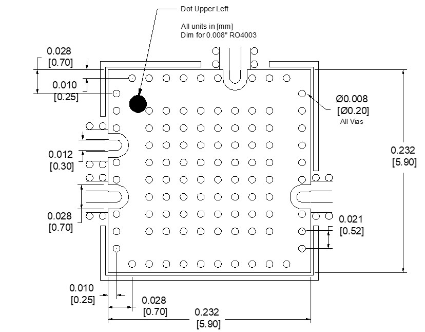
Download : Footprint Drawing
MMIQ-0218LSM-2
Broadband Drive Surface Mount MMIC IQ Mixer