Port Diagram
A top-down x-ray view of the MFBC-00015PSM package outline drawing is shown below. The MMIC bandpass filters are symmetrical allowing Pin 5 or Port 20 to be used as the input.


Sales: 408-778-9952 | General: 408-778-4200 | Fax: 408-778-4300
Sales & Customer Support: [email protected]
Tech Support: [email protected]
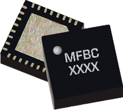
The MFBC-00015PSM family of passive MMIC surface mount bandpass filters are an ideal solution for small form factor, high rejection filtering. Passive GaAs MMIC technology allows production of smaller filter constructions that replace larger form factor circuit board constructions. Tight fabrication tolerances allow for less unit-to-unit variation than traditional filter technologies. The MFBC-000XXPSM is available as a 5x5mm plastic QFN. Low unit to unit variation allows for accurate simulations using the provided S2P file taken from measured production units.
N/A

| Part Number | Description | Package | Green Status | Product Lifecycle | Export Classification |
|---|---|---|---|---|---|
| MFBC-00015PSM | Passive GaAs MMIC 25.40 – 34.70 Bandpass Filter | QFN | RoHS REACH | Released | EAR99 |
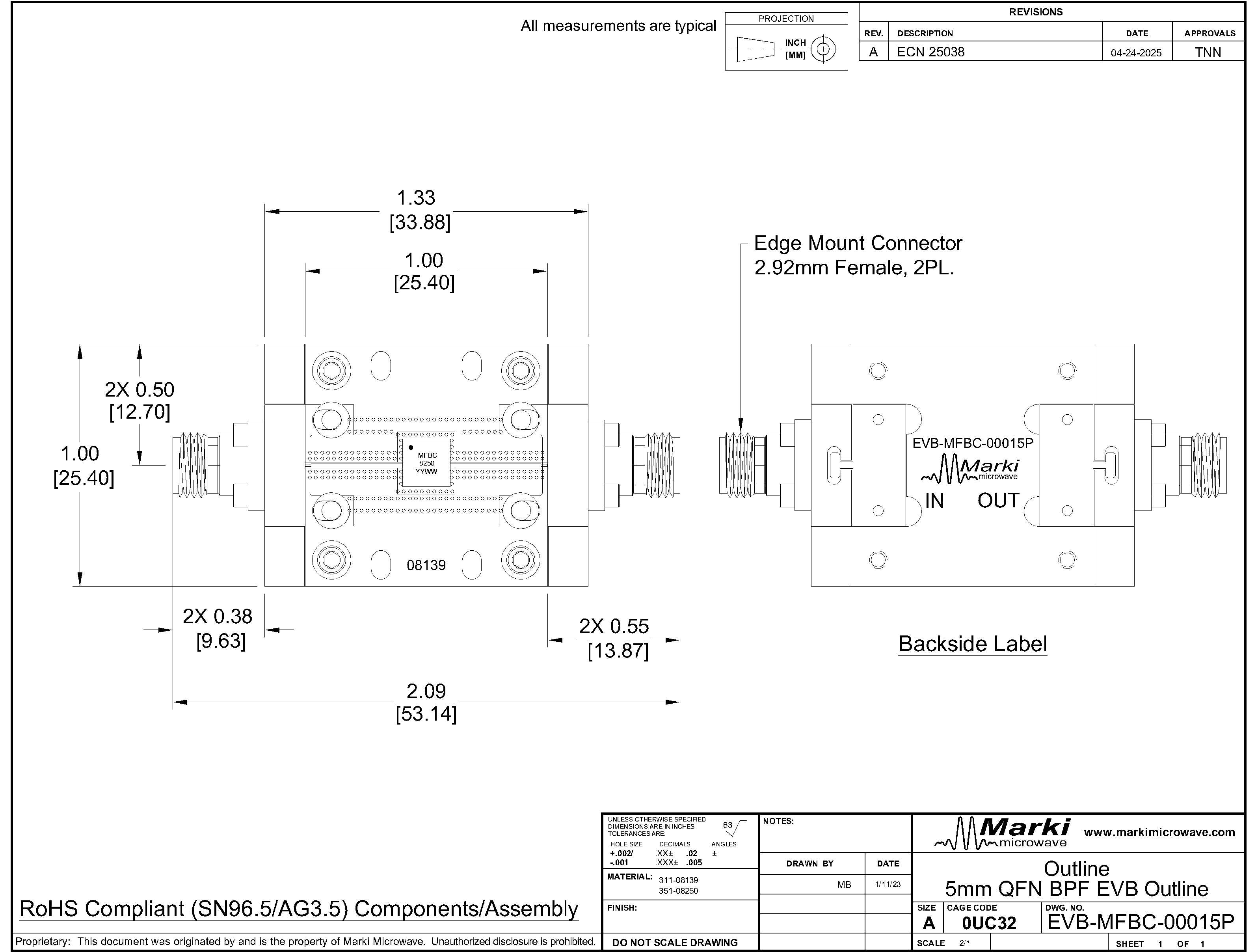
| EVB-MFBC-00015P | Evaluation Board, Passive GaAs MMIC 25.40 - 34.70 GHz Bandpass Filter | EVB | RoHS REACH | Released | EAR99 |
| Part Number | Description | Package | Green Status | Product Lifecycle | Export Classification |
|---|---|---|---|---|---|
| MFBC-00015PSM | Passive GaAs MMIC 25.40 – 34.70 Bandpass Filter | QFN | RoHS REACH | Released | EAR99 |
| EVB-MFBC-00015P | Evaluation Board, Passive GaAs MMIC 25.40 - 34.70 GHz Bandpass Filter | EVB | RoHS REACH | Released | EAR99 |
MFBC-00015PSM
Passive GaAs MMIC 25.40 – 34.70 Bandpass Filter
| Revision Code | Revision Date | Comment |
|---|---|---|
| - | 2022-12-01 | Datasheet Initial Release |
| A | 2023-02-01 | Added MFBC-00016PSM |
| B | 2023-04-01 | Added MFBC-00010PSM – MFBC-00015PSM |
MFBC-00015PSM
Passive GaAs MMIC 25.40 – 34.70 Bandpass Filter
A top-down x-ray view of the MFBC-00015PSM package outline drawing is shown below. The MMIC bandpass filters are symmetrical allowing Pin 5 or Port 20 to be used as the input.
| Port | Function | Description | DC Equivalent Circuit |
|---|---|---|---|
| Ground Paddle | Ground | PSM package ground path is provided through the ground paddle and should be connected to RF ground. |  |
| Pin 20 | Input/Output | Pin 20 is DC short to ground for the PSM package. |  |
| Pin 5 | Input/Output | Pin 5 is DC short to ground for the PSM package. | |
MFBC-00015PSM
Passive GaAs MMIC 25.40 – 34.70 Bandpass Filter
The Absolute Maximum Ratings indicate limits beyond which damage may occur to the device. If these limits are exceeded, the device may be inoperable or have a reduced lifetime.
| Parameter | Maximum Rating | Unit |
|---|---|---|
| Maximum Operating Temperature | 100 | °C |
| Maximum Storage Temperature | 125 | °C |
| Minimum Operating Temperature | -55 | °C |
| Minimum Storage Temperature | -65 | °C |
| Port 1 DC Current | 600 | mA |
| Port 2 DC Current | 600 | mA |
| Parameter | Details | Rating |
|---|---|---|
| Dimensions | - | 5 x 5 mm |
| Moisture Sensitivity Level | - | MSL 1 |
MFBC-00015PSM
Passive GaAs MMIC 25.40 – 34.70 Bandpass Filter
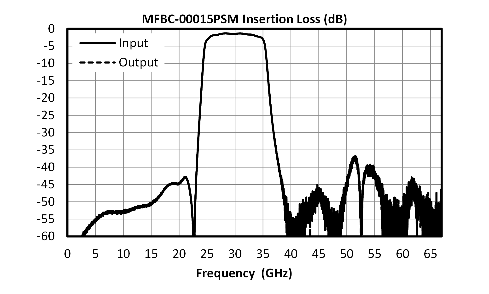
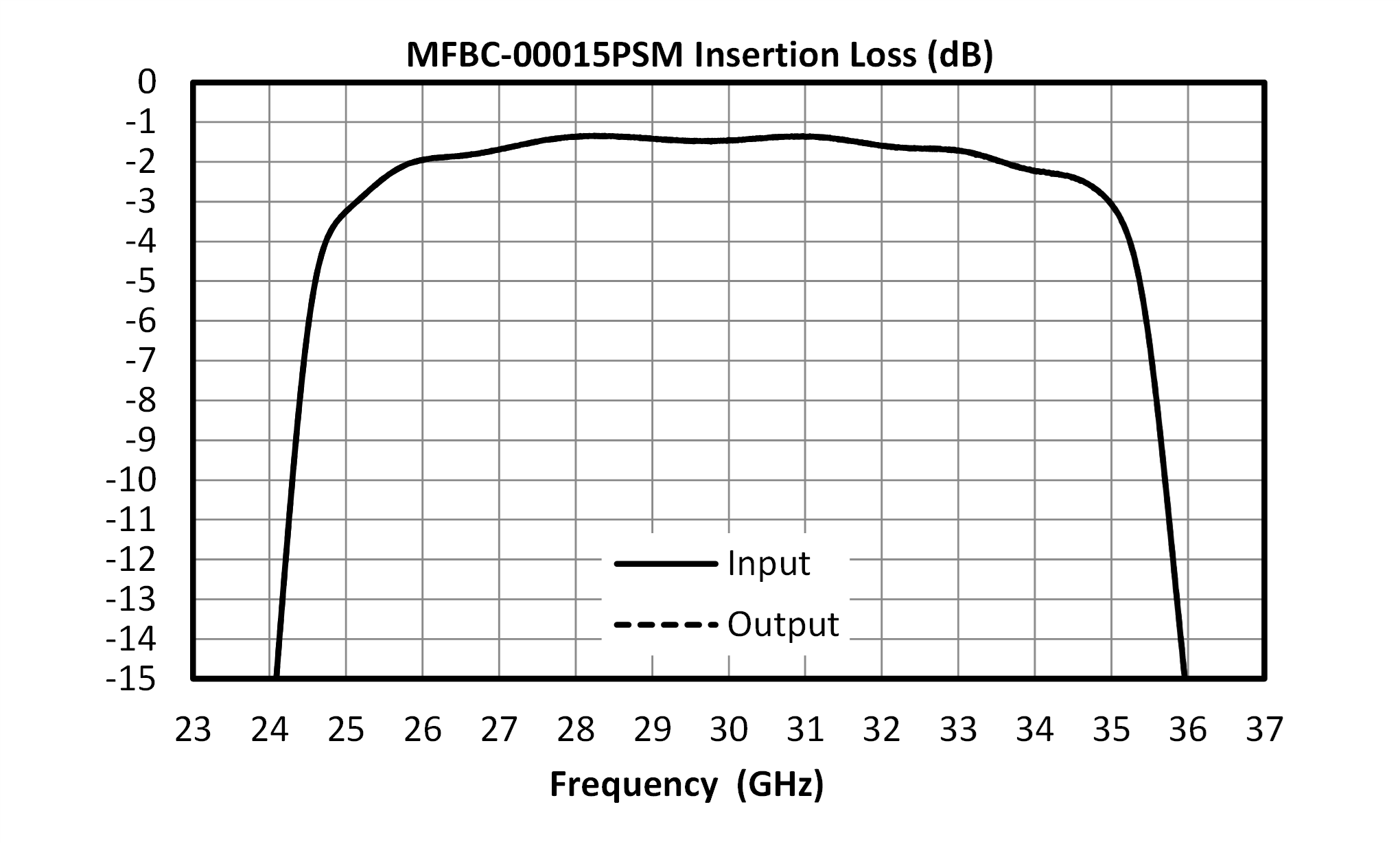
The electrical specifications apply at TA=+25°C in a 50Ω system. Typical data shown is for the filter in a PSM package with a sine wave input applied to Pin 5. Min and Max limits are guaranteed at TA=+25°C.
| Parameter | Test Conditions | Minimum Frequency (GHz) | Maximum Frequency (GHz) | Min | Typ | Max | Unit |
|---|---|---|---|---|---|---|---|
| 1 dBc Passband | Temp = 25°C | 25.46 | 34.64 | - | - | - | GHz |
| 3 dBc Passband | Temp = 25°C | 24.54 | 35.41 | - | - | - | GHz |
| 30 dBc Rejection Point | Temp = 25°C | 23.2 | 37.12 | - | - | - | GHz |
| Center Freq | Temp = 25°C | - | - | - | 29.70 | - | GHz |
| Insertion Loss @ fc | Temp = 25°C | - | - | - | 1.5 | - | dB |
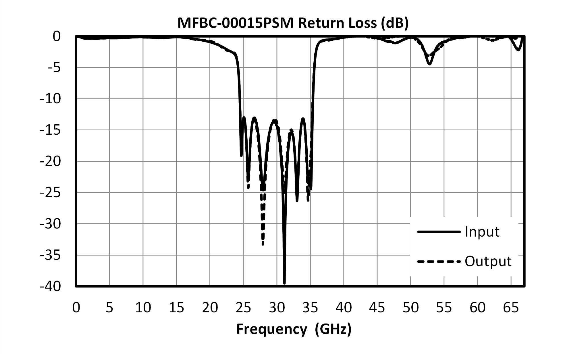
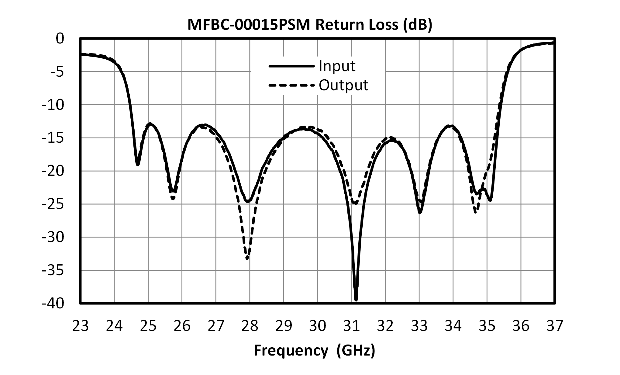
| Passband Return Loss | Temp = 25°C | - | - | - | 18 | - | dB |
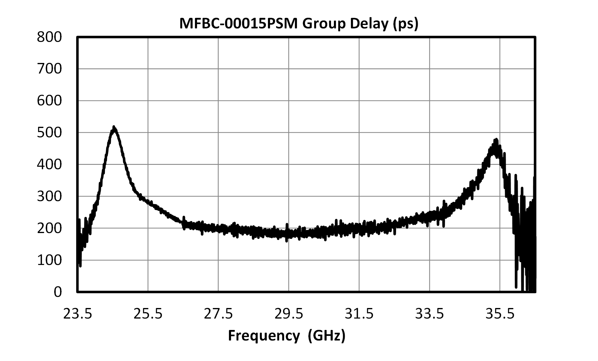
| Group Delay | Temp = 25°C | - | - | - | 198 | - | ps |
| Impedance | Temp = 25°C | - | - | - | 50 | - | Ω |
| Stopband Suppression | - | 0 | 21 | 40 | 70 | - | dB |
| Stopband Suppression | - | 38 | 67 | 30 | 45 | - | dB |
| Parameter | Test Conditions | Minimum Frequency (GHz) | Maximum Frequency (GHz) | Min | Typ | Max | Unit |
|---|---|---|---|---|---|---|---|
| 1 dBc Passband | Temp = 25°C | 25.46 | 34.64 | - | - | - | GHz |
| 3 dBc Passband | Temp = 25°C | 24.54 | 35.41 | - | - | - | GHz |
| 30 dBc Rejection Point | Temp = 25°C | 23.2 | 37.12 | - | - | - | GHz |
| Center Freq | Temp = 25°C | - | - | - | 29.70 | - | GHz |
| Insertion Loss @ fc | Temp = 25°C | - | - | - | 1.5 | - | dB |
| Passband Return Loss | Temp = 25°C | - | - | - | 18 | - | dB |
| Group Delay | Temp = 25°C | - | - | - | 198 | - | ps |
| Impedance | Temp = 25°C | - | - | - | 50 | - | Ω |
| Stopband Suppression | - | 0 | 21 | 40 | 70 | - | dB |
| Stopband Suppression | - | 38 | 67 | 30 | 45 | - | dB |
MFBC-00015PSM
Passive GaAs MMIC 25.40 – 34.70 Bandpass Filter
MFBC-00015PSM
Passive GaAs MMIC 25.40 – 34.70 Bandpass Filter
Download : Outline 2D Drawing Outline 3D Drawing Outline 3D STP

Notes (unless otherwise specified):
MFBC-00015PSM
Passive GaAs MMIC 25.40 – 34.70 Bandpass Filter
Download : Footprint Drawing

MFBC-00015PSM
Passive GaAs MMIC 25.40 – 34.70 Bandpass Filter