Port Diagram
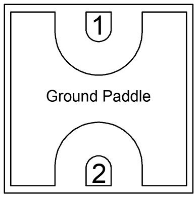
An x-ray view of the MEQ9-40CSP1 package outline drawing is shown below. The MEQ equalizers are symmetrical allowing Port 1 or Port 2 to be used as the input.
Sales: 408-778-9952 | General: 408-778-4200 | Fax: 408-778-4300
Sales & Customer Support: [email protected]
Tech Support: [email protected]
The MEQ9-40CSP1 is a passive MMIC equalizer in our compact 1.5mm CSP1 chip scale surface mount package. The MEQ9-40CSP1 provides a positive slope equalization from DC-40 GHz with a DC attenuation of 9 dB, and achieves a 23 dB return loss all in a compact form factor. The chip scale package allows for extreme miniaturization of the SMT footprint while maintaining standard solder reflow processes. Designed for RF systems that prioritize SWAP, this equalizer compensates for frequency-dependent losses and improves gain flatness across broadband signal chains. Common applications include compensating for high frequency amplifier gain roll off, equalizing filter passbands, and improving the eye diagram in high-speed digital systems.


| Part Number | Description | Package | Green Status | Product Lifecycle | Export Classification |
|---|---|---|---|---|---|
| MEQ9-40CSP1 | Chip Scale Package MMIC DC-40 GHz 9 dB Equalizer | CSP1 | REACH RoHS | Released | EAR99 |
| EVB-MEQ9-40 | Evaluation Board, Chip Scale Package MMIC DC-40 GHz 9 dB Equalizer | EVB | REACH RoHS | Released | EAR99 |
MEQ9-40CSP1
Chip Scale Package MMIC DC-40 GHz 9 dB Equalizer
| Revision Code | Revision Date | Comment |
|---|---|---|
| - | 2025-08-13 | Initial Release |
MEQ9-40CSP1
Chip Scale Package MMIC DC-40 GHz 9 dB Equalizer
An x-ray view of the MEQ9-40CSP1 package outline drawing is shown below. The MEQ equalizers are symmetrical allowing Port 1 or Port 2 to be used as the input.
| Port | Function | Description | DC Equivalent Circuit |
|---|---|---|---|
| GND | Ground | SM package ground path is provided through the ground paddle. |  |
| Pin 1 | Input/Output | Pin 1 is DC connected to ground through a resistor. DC block is required if voltage present. |  |
| Pin 2 | Input/Output | Pin 2 is DC connected to ground through a resistor. DC block is required if voltage present. |  |
MEQ9-40CSP1
Chip Scale Package MMIC DC-40 GHz 9 dB Equalizer
The Absolute Maximum Ratings indicate limits beyond which damage may occur to the device. If these limits are exceeded, the device may be inoperable or have a reduced lifetime.
| Parameter | Maximum Rating | Unit |
|---|---|---|
| Maximum Operating Temperature | 100 | °C |
| Maximum Storage Temperature | 125 | °C |
| Minimum Operating Temperature | -55 | °C |
| Minimum Storage Temperature | -65 | °C |
| Port 1 DC Current | 25 | mA |
| Port 2 DC Current | 25 | mA |
| Power Handling, at any Port (25°C) | 30 | dBm |
| Parameter | Details | Rating |
|---|---|---|
| ESD | 250 to < 500 Volts | HBM Class 1A |
| Weight | Package name: CSP1 | 0.04g |
| Dimensions | - | 1.50 x 1.50 mm |
| Moisture Sensitivity Level | - | MSL 3 |
MEQ9-40CSP1
Chip Scale Package MMIC DC-40 GHz 9 dB Equalizer
The electrical specifications apply at TA=+25°C in a 50Ω system. Typical data shown is for the equalizer in a CSP1 package with a sine wave input applied to port 1. Min and Max limits are guaranteed at TA=+25°C.
| Parameter | Test Conditions | Minimum Frequency (GHz) | Maximum Frequency (GHz) | Min | Typ | Max | Unit |
|---|---|---|---|---|---|---|---|
| Insertion Loss at DC | Temp = 25°C | 0 | 0 | - | 9.1 | - | dB |
| Insertion Loss | Temp = 25°C | 20 | 20 | - | 4.3 | - | dB |
| Insertion Loss | Temp = 25°C | 40 | 40 | - | 0.8 | - | dB |
| Equalization Value | Temp = 25°C | 0 | 40 | - | 8.3 | - | dB |
| Return Loss | Temp = 25°C | 0 | 40 | - | 23 | - | dB |
| Group Delay | Temp = 25°C | 0 | 40 | - | 16 | - | ps |
Equalizer is symmetrical. Reverse measurement is equivalent to forward measurement. All measurements taken in EVB package and de-embedded to the CSP1 pad interface.
MEQ9-40CSP1
Chip Scale Package MMIC DC-40 GHz 9 dB Equalizer
.png)
.png)
.png)
MEQ9-40CSP1
Chip Scale Package MMIC DC-40 GHz 9 dB Equalizer
MEQ9-40CSP1
Chip Scale Package MMIC DC-40 GHz 9 dB Equalizer
Download : Footprint Drawing

MEQ9-40CSP1
Chip Scale Package MMIC DC-40 GHz 9 dB Equalizer

