Port Diagram
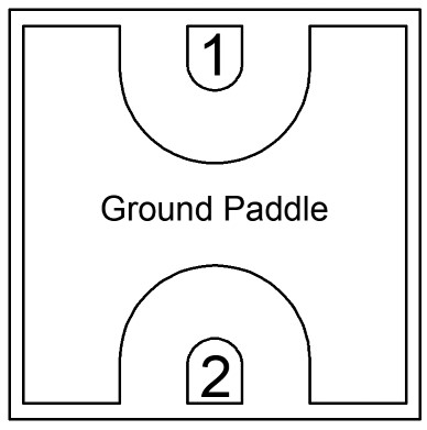
An x-ray view of the MEQ10-26CSP1 package outline drawing is shown below. The MEQ equalizers are symmetrical allowing Port 1 or Port 2 to be used as the input.
Sales: 408-778-9952 | General: 408-778-4200 | Fax: 408-778-4300
Sales & Customer Support: [email protected]
Tech Support: [email protected]
The MEQ10-26CSP1 is a passive MMIC equalizer CSP ideal for compensating for low pass filtering effects in RF/microwave and high speed digital systems. The MEQ10-26CSP1 provides positive slope from DC to 26GHz with a DC attenuation of 10dB. The chip scale package allows for extreme miniaturization of the SMT footprint. The unique design offers superior return loss to competitors in an extremely small footprint. GaAs MMIC technology provides consistent unit-to-unit performance in a small, low cost form factor.


| Part Number | Description | Package | Green Status | Product Lifecycle | Export Classification |
|---|---|---|---|---|---|
| MEQ10-26CSP1 | Chip Scale Package MMIC 26 GHz Equalizer | CSP1 | REACH RoHS | Released | EAR99 |
| EVB-MEQ10-26 | Evaluation Board, Chip Scale Package MMIC 26 GHz Equalizer | EVB | REACH RoHS | Released | - |
MEQ10-26CSP1
Chip Scale Package MMIC 26 GHz Equalizer
| Revision Code | Revision Date | Comment |
|---|---|---|
| - | 2022-07-01 | Datasheet Initial Release |
| A | 2023-02-01 | Package Description Updated |
MEQ10-26CSP1
Chip Scale Package MMIC 26 GHz Equalizer
An x-ray view of the MEQ10-26CSP1 package outline drawing is shown below. The MEQ equalizers are symmetrical allowing Port 1 or Port 2 to be used as the input.
| Port | Function | Description | DC Equivalent Circuit |
|---|---|---|---|
| GND | Ground | SM package ground path is provided through the ground paddle. |  |
| Pin 1 | Input/Output | Pin 1 is DC connected to ground through a resistor. DC block is required if voltage present. |  |
| Pin 2 | Input/Output | Pin 2 is DC connected to ground through a resistor. DC block is required if voltage present. |  |
MEQ10-26CSP1
Chip Scale Package MMIC 26 GHz Equalizer
The Absolute Maximum Ratings indicate limits beyond which damage may occur to the device. If these limits are exceeded, the device may be inoperable or have a reduced lifetime.
| Parameter | Maximum Rating | Unit |
|---|---|---|
| Maximum Operating Temperature | 100 | °C |
| Maximum Storage Temperature | 125 | °C |
| Minimum Operating Temperature | -55 | °C |
| Minimum Storage Temperature | -65 | °C |
| Power Handling, at any Port | 2 | W |
| Parameter | Details | Rating |
|---|---|---|
| ESD | 250 to < 500 Volts | HBM Class 1A |
| Dimensions | - | 1.5 x 1.5 mm |
| Moisture Sensitivity Level | - | MSL 3 |
MEQ10-26CSP1
Chip Scale Package MMIC 26 GHz Equalizer
The electrical specifications apply at TA=+25°C in a 50Ω system. Typical data shown is for the equalizer in a CSP package with a sine wave input applied to port 1. Min and Max limits are guaranteed at TA=+25°C. All bare die are 100% DC tested and visually inspected.
| Parameter | Test Conditions | Minimum Frequency (GHz) | Maximum Frequency (GHz) | Min | Typ | Max | Unit |
|---|---|---|---|---|---|---|---|
| Impedance | - | 0 | 26 | - | 50 | - | Ω |
| Insertion Loss | - | 26 | 26 | - | 0.75 | - | dB |
| Insertion Loss at DC | - | 0 | 0 | - | 10 | - | dB |
| Return Loss | - | 0 | 26 | - | 17 | - | dB |
Equalizer is symmetrical. Reverse measurement is equivalent to forward measurement. All measurements taken in EVB package and de-embedded to the CSP1 pad interface.
MEQ10-26CSP1
Chip Scale Package MMIC 26 GHz Equalizer


MEQ10-26CSP1
Chip Scale Package MMIC 26 GHz Equalizer
MEQ10-26CSP1
Chip Scale Package MMIC 26 GHz Equalizer
Download : Footprint Drawing

MEQ10-26CSP1
Chip Scale Package MMIC 26 GHz Equalizer

