Rev: A | Copyright © 2023, 2025 Marki Microwave LLC.

General Description

The BTM-0026PSM-2 is a packaged miniature bias tee featuring excellent 0.4 dB insertion loss and superior 25 dB isolations over a broad 10 MHz to 26 GHz bandwidth. The BTM-0026PSM-2 works well for K-Band applications. The BTM-0026PSM-2 is available in a compact 2.25 x 3.7 mm surface mount package or as a connectorized evaluation board. Tight fabrication tolerances allow for low unit to unit variation enabling accurate simulations using the provided s3p file taken from measured production units, making it an excellent alternative to uncharacterized, untested bias tees built with off-the-shelf inductors and capacitors.

Features

  • Low 0.4 dB Insertion Loss
  • 16 V Voltage & 0.32 A Current Rating
  • 1 W Power Handling
  • Miniature Surface Mount Package
  • Broad 10MHz to 26GHz Bandwidth

Functional Block Diagram

Block Diagram
Photo of BTM-0026PSM-2

Electrical Performance Summary

ParameterTypUnit
Frequency Range0.01 to 26GHz
DC Current 0.32A
DC Voltage 16V
Insertion Loss 0.43dB
DC Port Isolation 25dB

Summary only – refer to the Electrical Specifications, Absolute Maximum Ratings, and Recommended Operating Range tables for complete details.

Part Ordering Options

Part NumberDescriptionPackageGreen StatusProduct LifecycleExport Classification
BTM-0026PSM-1Miniature Surface Mount 0.01 - 26 GHz Bias-TeePSM

RoHS

REACH

ReleasedEAR99
BTM-0026PSM-2Miniature Surface Mount 0.01 - 26 GHz Bias-TeePSM

RoHS

REACH

ReleasedEAR99
EVB-BTM-0026PEvaluation Board, Miniature Surface Mount 0.01 - 26 GHz Bias-TeeEVB

RoHS

REACH

ReleasedEAR99

Table Of Contents

Typical Performance Plots

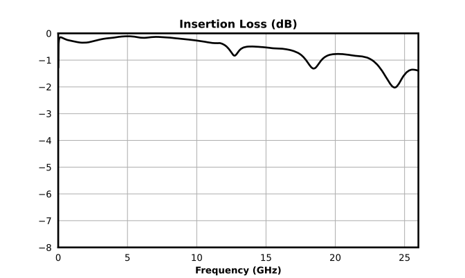
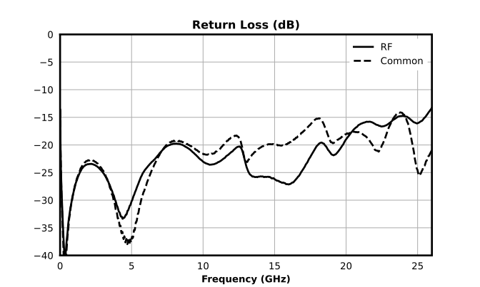
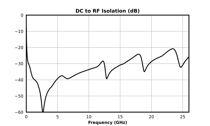
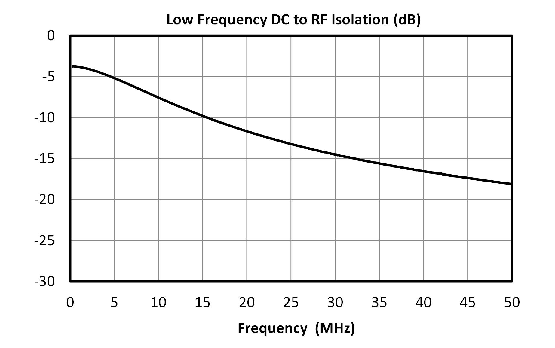
Typical performance plots are evaluation board measurements with fixturing to the device pads de-embedded except for low frequency plots.

Insertion Loss (dB) graph for BTM-0026PSM-2
Return Loss (dB) graph for BTM-0026PSM-2
DC to RF Isolation (dB) graph for BTM-0026PSM-2
Low Frequency DC to RF Isolation (dB) graph for BTM-0026PSM-2
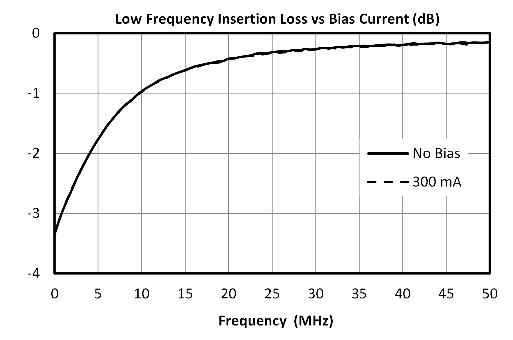
Low Frequency Insertion Loss vs Bias Current graph for BTM-0026PSM-2
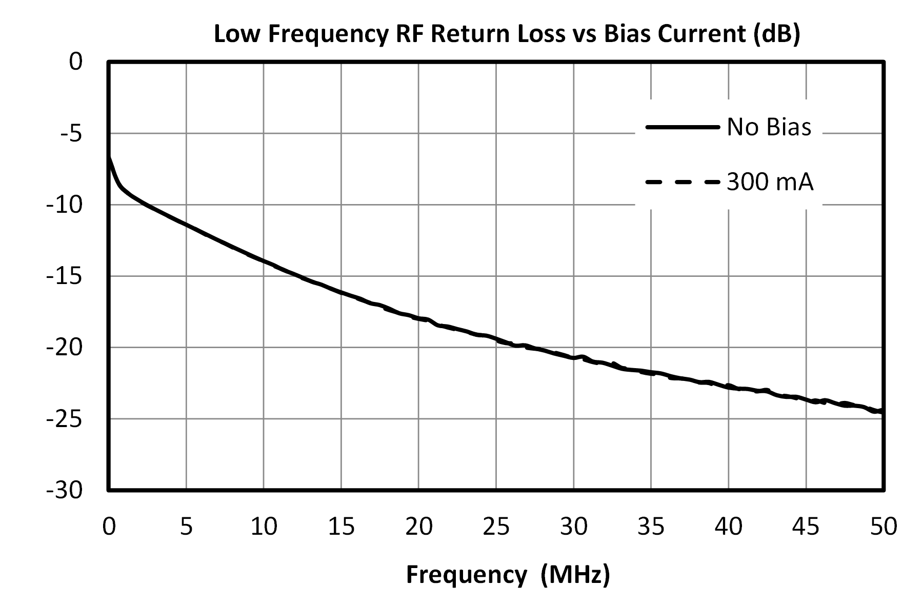
Low Frequency RF Return Loss vs Bias Current (dB) graph for BTM-0026PSM-2
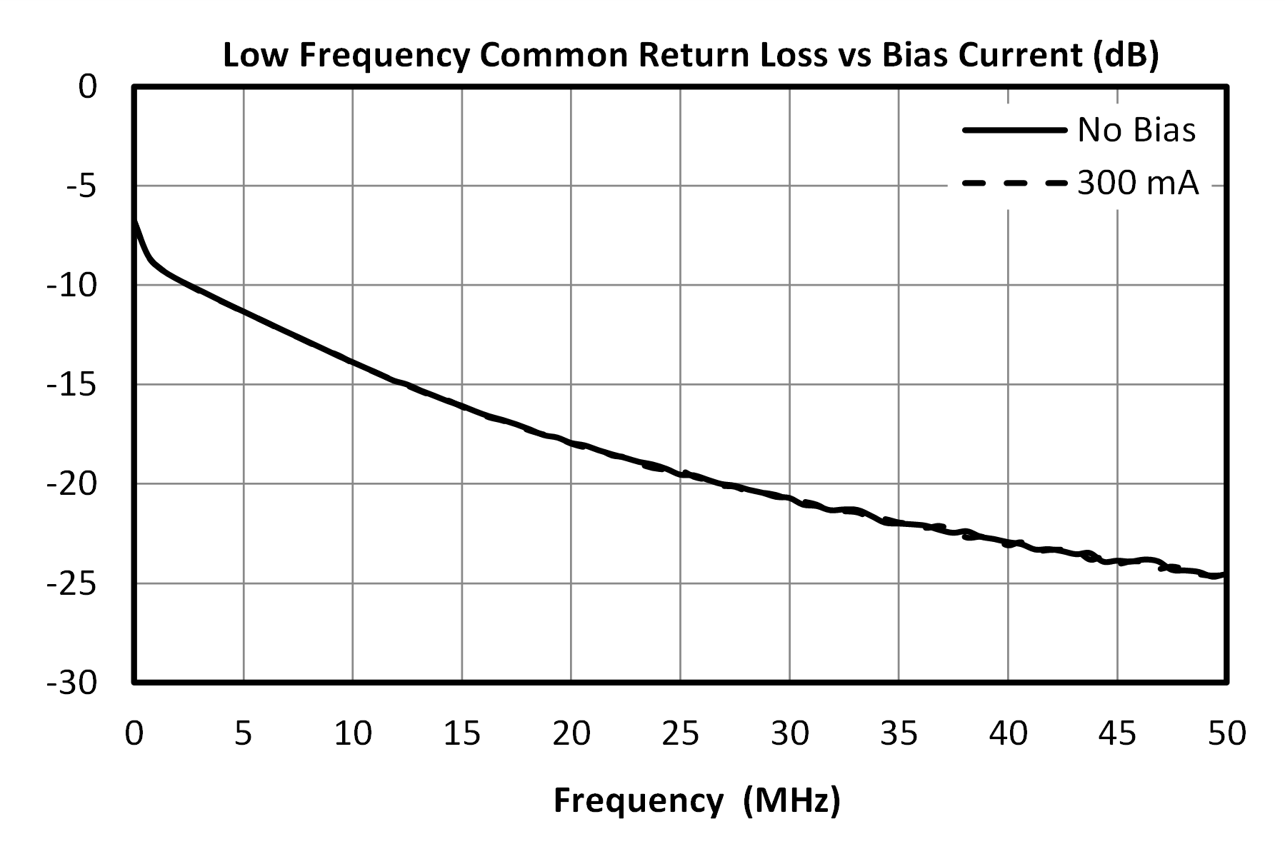
Low Frequency Common Return Loss vs Bias Current (dB) graph for BTM-0026PSM-2

Specifications

Electrical Specifications

Specifications guaranteed at +25C, measured in a 50-Ohm system

ParameterTest ConditionsMinimum
Frequency
(GHz)
Maximum
Frequency
(GHz)
MinTypMaxUnit
Frequency Range-0.01 26---GHz
Capacitance -0.01 26-0.1-μF
DC Port Isolation -0.01 26-25-dB
DC Resistance -0.01 26-1.5-Ω
Impedance -0.01 26-50-Ω
Inductance -0.01 26-1.1-μH
Insertion Loss -0.01 26-0.432.5dB
Return Loss -0.01 26-20-dB

Absolute Maximum Ratings

The Absolute Maximum Ratings indicate limits beyond which damage may occur to the device. If these limits are exceeded or met simultaneously, the device may be inoperable or have a reduced lifetime.

ParameterMaximum RatingUnit
Power Handling 30dBm
DC Voltage 16V
DC Current 0.32A
Minimum Operating Temperature -55°C
Minimum Storage Temperature -65°C
Maximum Operating Temperature 100°C
Maximum Storage Temperature 125°C

Package Information

ParameterDetailsRating
ESD250 to < 500 VoltsHBM Class 1A
WeightPackage name: PSM0.69g
Dimensions-2.25 x 3.70 mm
Moisture Sensitivity Level-MSL 1

Port Configuration and Functions

Port Diagram

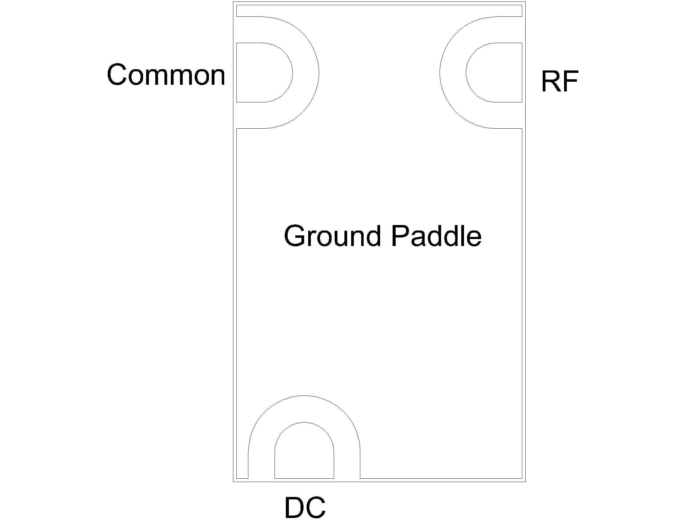
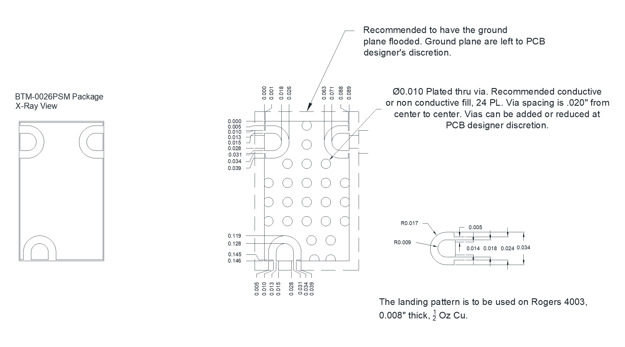
A top-down x-ray view of the BTM-0026PSM-2’s PSM package outline drawing is shown below. The BTM-0026PSM-2 has input and output ports given in Port Functions below. To use, apply a DC voltage to the DC pin, and an RF signal to the RF pin.

Diagram of the port configuration for BTM-0026PSM-2

Port Functions

PortFunctionDescriptionDC Equivalent
Circuit
CommonRF+DC The Common port is AC coupled to the RF pin and DC coupled to the DC pin.Equivalent circuit for the RF+DC
DCDC The DC port is DC blocked to the RF pin and DC coupled to the common port.Equivalent circuit for the DC
RFRF The RF pin is AC coupled to the common pin and DC blocked to the DC pin.Equivalent circuit for the RF

Mechanical Data

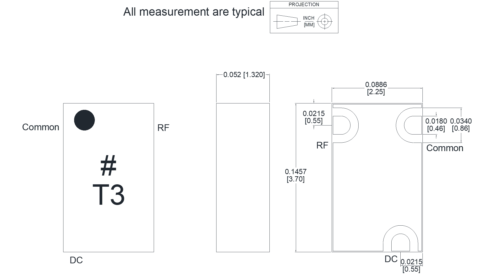
Outline Drawing

Download : Outline 2D Drawing Outline 3D Drawing Outline 3D STP

Outline Drawing

Notes: (Unless otherwise specified)

All dimensions are in INCHES [MM].

Finish: Gold 2-8µ-inches, over Solderable Electroplated Nickel, 100-200 µ-inches per QQ-N-290A. Or, ENIG.

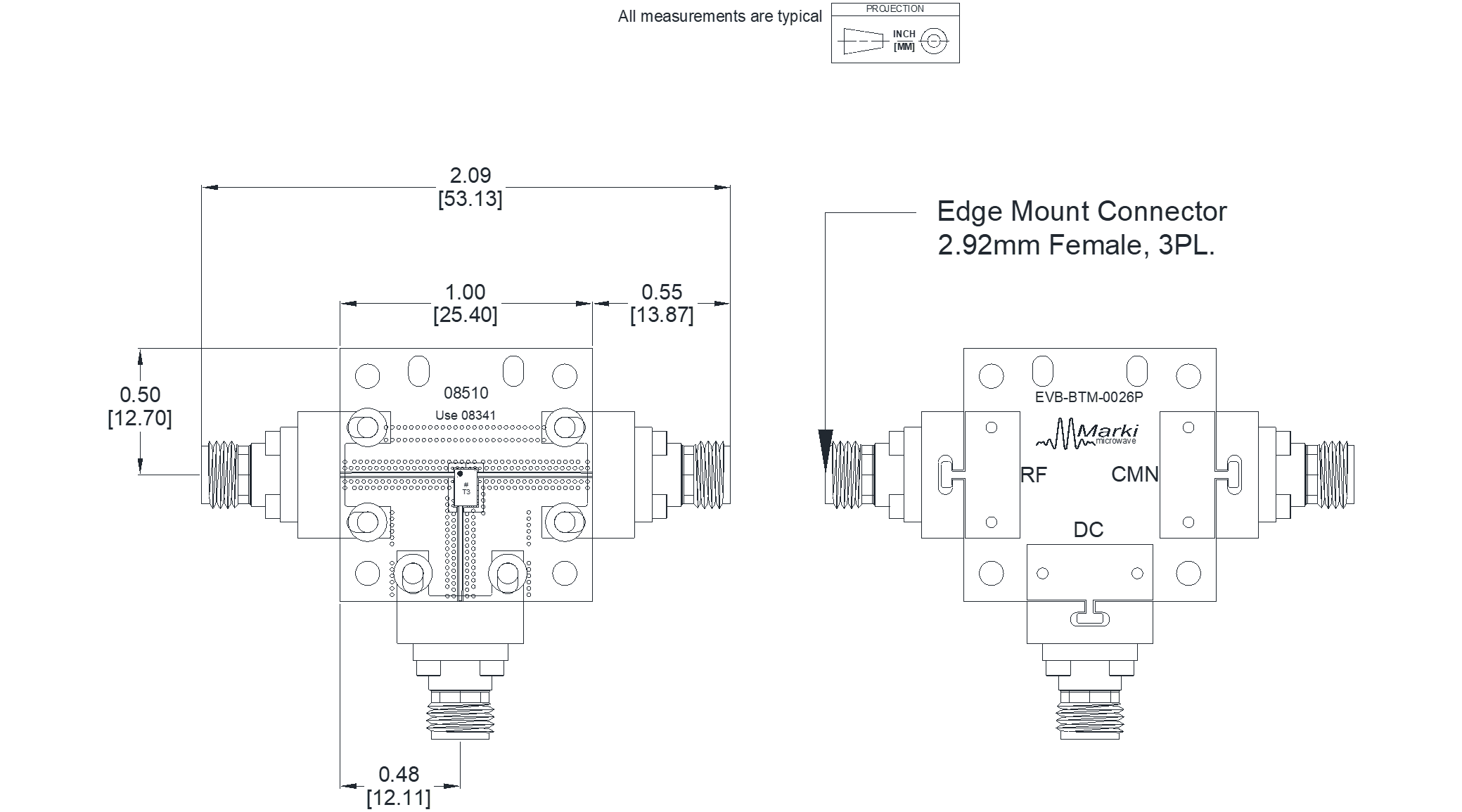
Evaluation Board

Evaluation Board - Outline Drawing

Outline Drawing

Revision History

Revision CodeRevision DateComment
-2023-03-01Datasheet Initial Release
A2025-02-10Updates as per ECN 25013

DISCLAIMER

MARKI MICROWAVE, LLC., (“MARKI”) PROVIDES TECHNICAL SPECIFICATIONS AND DATA (INCLUDING DATASHEETS), APPLICATION OR OTHER DESIGN ADVICE, WEB TOOLS, AND OTHER INFORMATION AND RESOURCES “AS IS” AND WITH ALL FAULTS. MARKI DISCLAIMS ALL WARRANTIES, EXPRESS OR IMPLIED, INCLUDING, WITHOUT LIMITATION, ANY IMPLIED WARRANTIES OF MERCHANTABILITY, FITNESS FOR A PARTICULAR PURPOSE, OR NON-INFRINGEMENT.

These resources are intended for developers skilled in the art designing with Marki products. You are solely responsible for (1) selecting the appropriate products for your application, (2) designing, validating, and testing your application, and (3) ensuring your application meets applicable standards and other requirements. Marki makes no guarantee regarding the suitability of its products for any particular purpose, nor does Marki assume any liability whatsoever arising out of your use or application of any Marki product.

Marki grants you permission to use these resources only for development of an application that uses Marki products. Other reproduction or use of these resources is strictly prohibited. No license is granted to any other Marki intellectual property or to any third-party intellectual property. Marki reserves the right to make changes to the product(s) or information contained herein without notice.

MARKI MICROWAVE, M wave logo, FastSwitch, and T3 MIXER are trademarks or registered trademarks of Marki Microwave, LLC. All other trademarks used are the property of their respective owners.

© 2023, 2025, Marki Microwave, LLC